Semiconductor laser device and method of manufacturing the same

a laser device and semiconductor technology, applied in the direction of lasers, laser optical resonators, semiconductor lasers, etc., can solve the problems of disadvantageous damage of the ridge portion b>102/b>/i>(waveguide), and suppress the bonding of metal wires to the waveguide, so as to suppress the deterioration of laser characteristics, suppress the bonding, and suppress the effect of metal wire bonding

Inactive Publication Date: 2011-03-08
SANYO ELECTRIC CO LTD
View PDF12 Cites 1 Cited by
  • Summary
  • Abstract
  • Description
  • Claims
  • Application Information

AI Technical Summary

Benefits of technology

[0014]In the semiconductor laser device according to the first aspect, as hereinabove described, the waveguide extending in the prescribed direction (first direction parallel to the surface of the substrate) is formed on the region approaching the first side from the center of the semiconductor layer in the second direction parallel to the surface of the substrate and intersecting with the first direction. Thus, bonding of a metal wire onto the waveguide can be suppressed in a case of bonding the metal wire to the center of an upper surface of the semiconductor layer for supplying power to the upper surface of the semiconductor layer, whereby damage of the waveguide can be suppressed in bonding. Consequently, deterioration of the laser characteristics can be suppressed.
[0022]The method of manufacturing a semiconductor laser device comprises a step of forming the plurality of first recess portions between the plurality of waveguides from the side of the semiconductor layer so as to intersect with the first regions and to extend in the second direction intersecting with the extensional first direction of the waveguides. In other words, the method of manufacturing a semiconductor laser device comprises a step of forming the plurality of first recess portions intersecting with the first regions and extending in the second direction parallel to the surface and intersecting with the first direction from the side of the upper surface of the semiconductor layer. Thus, the first recess portions can be formed on the positions separated from the waveguides and hence damage of the waveguides can be suppressed when the first recess portions are formed from the side of the upper surface of the semiconductor layer. Thus, deterioration of the laser characteristics of the device can be suppressed also by this.

Problems solved by technology

Therefore, the ridge portion 102a (waveguide) is disadvantageously damaged in bonding of the metal wire 108 to deteriorate laser characteristics.
Therefore, the ridge portion 102a (waveguide) is disadvantageously damaged.

Method used


Image

  • Semiconductor laser device and method of manufacturing the same
  • Semiconductor laser device and method of manufacturing the same
  • Semiconductor laser device and method of manufacturing the same

Examples


first embodiment

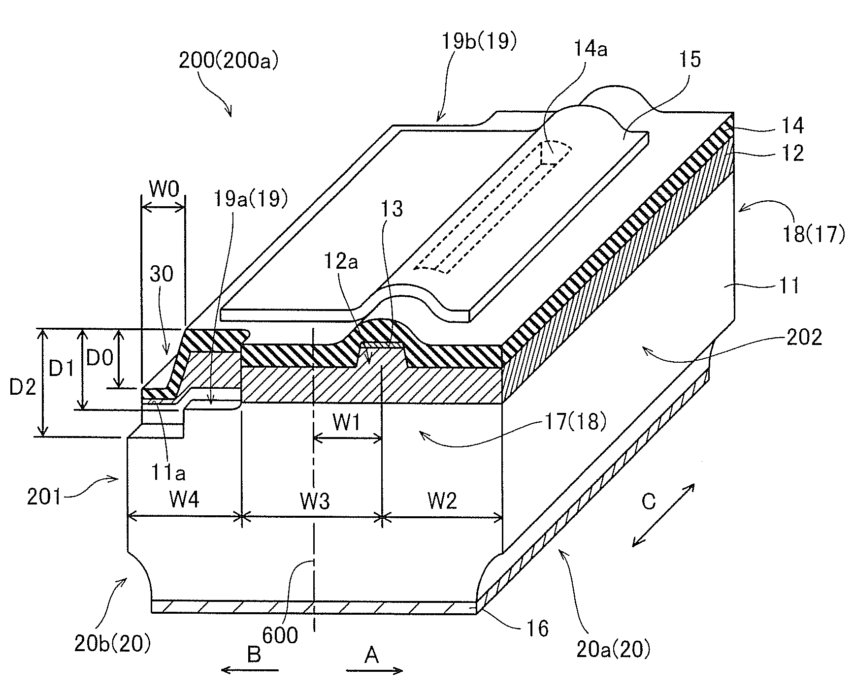
[0068]The structure of a GaN-based semiconductor laser chip (device) 200 according to a first embodiment will be now described with reference to FIGS. 4 and 5. The GaN-based semiconductor laser chip 200 according to the first embodiment is a 400 nm-band semiconductor laser chip (violet laser diode).

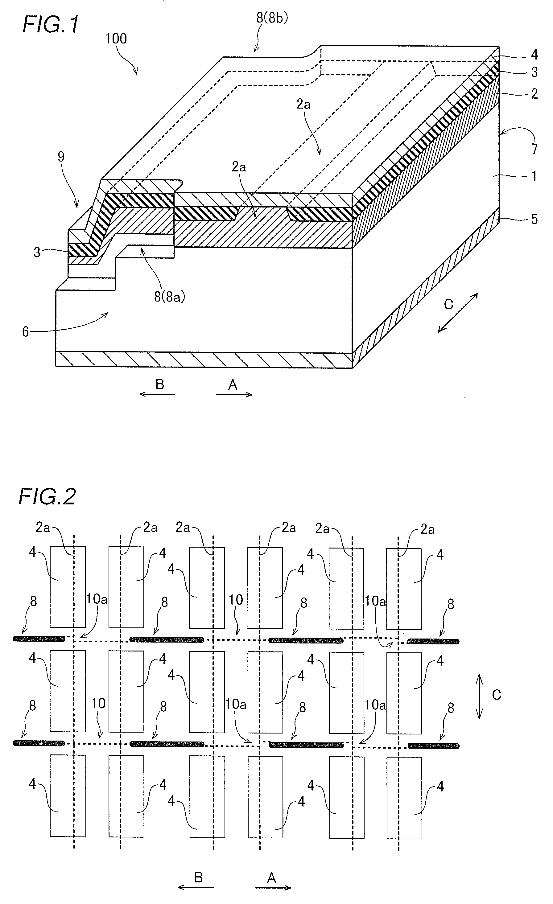
[0069]In the GaN-based semiconductor laser chip 200 according to the first embodiment, a semiconductor layer 12 including an active layer 24 (see FIG. 5) described later and having a p-n junction is formed on a substrate 11 made of n-type GaN, as shown in FIG. 4. This semiconductor layer 12 includes a ridge portion 12a constituting a waveguide extending in a direction C in a striped (slender) manner. The direction C is a laser emission direction of the GaN-based semiconductor laser chip 200 and is an example of the “first direction” in the present invention. The ridge portion 12a is an example of the “waveguide” in the present invention.

[0070]The GaN-based semiconductor laser chip 200 has...

first modification

of First Embodiment

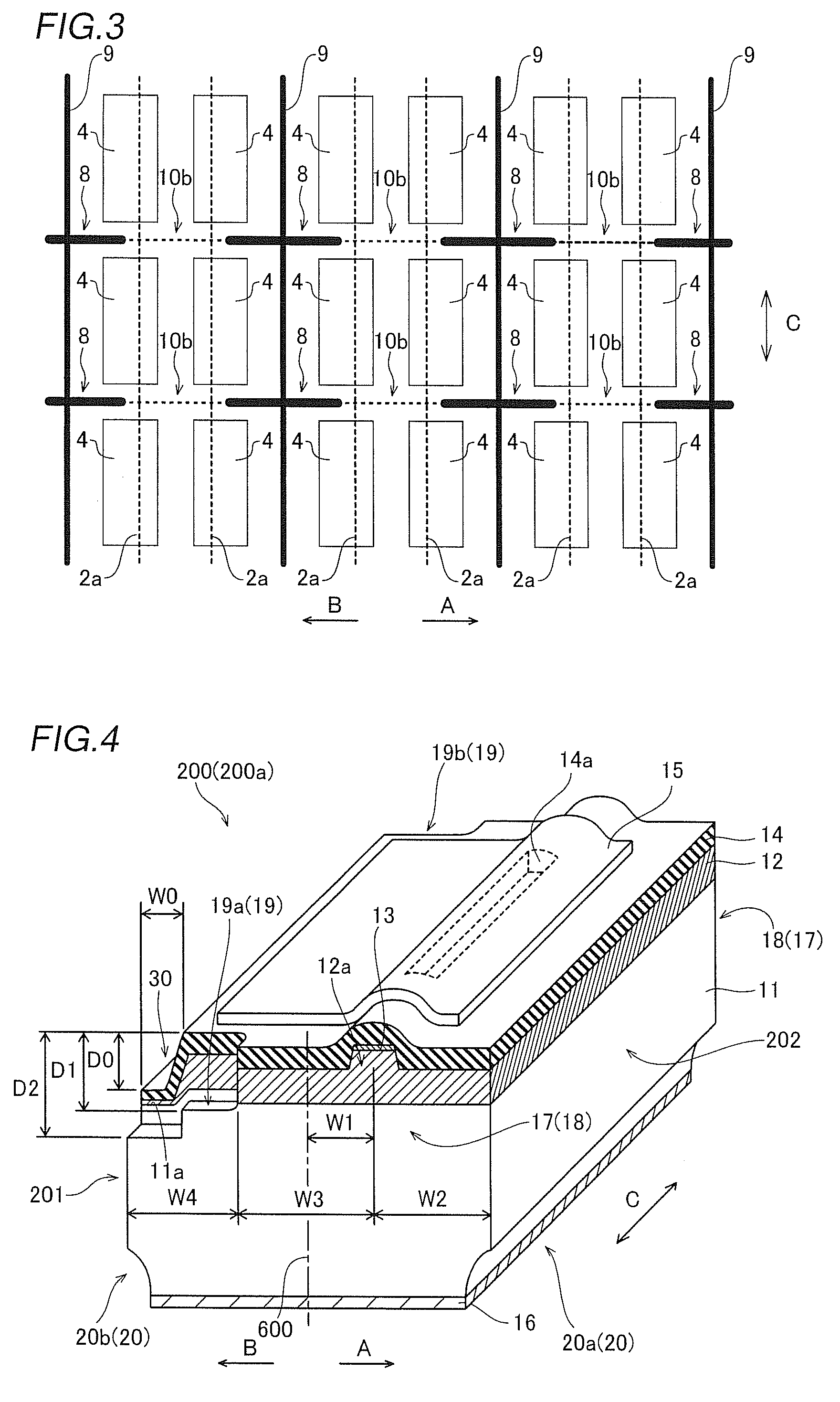
[0134]Referring to FIG. 13, in a GaN-based semiconductor laser chip 205 according to a first modification of the first embodiment, cleavage introduction steps 19a and 19b having depths not reaching a substrate 11 are formed on a semiconductor layer 12 dissimilarly to the aforementioned first embodiment. The cleavage introduction steps 19a and 19b are examples of the “first recess portion” in the present invention.

[0135]In the GaN-based semiconductor laser chip (device) 205 according to the first modification of the first embodiment, cleavage introduction steps 19c and 19d for performing cleavage having depths D11 (about 15 μm) are formed on boundaries between the cleavages 17 and 18 in the semiconductor layer 12 and a current blocking layer 14 from an upper surface of the GaN-based semiconductor laser chip 205, as shown in FIG. 13. In other words, in a separation process of the GaN-based semiconductor laser chip 205, the cleavage introduction steps 19c and 19d are...

second modification

of First Embodiment

[0137]Referring to FIGS. 12, 14 and 15, in a GaN-based semiconductor laser device according to a second modification of the first embodiment, three GaN-based semiconductor laser chips (devices) 210, 210a and 210b are obtained between a separation introduction recess portion 20 on a position opposed to one groove portion 30 and a separation introduction recess portion 20 adjacent thereto along arrow A (along arrow B) by separation, dissimilarly to the manufacturing process of the aforementioned first embodiment.

[0138]The GaN-based semiconductor laser chip according to the second modification of the first embodiment is so formed that one GaN-based semiconductor laser chip 210b is obtained in addition to the GaN-based semiconductor laser chip 210 (210a) having a device structure similar to that of the aforementioned first embodiment, as shown in FIG. 14. A ridge portion 12a of the GaN-based semiconductor laser chip 210b is formed on a region approaching a first side ...


PUM


Abstract

A semiconductor laser device includes a substrate and a semiconductor layer formed on a surface of the substrate and having a waveguide extending in a first direction parallel to the surface, wherein the waveguide is formed on a region approaching a first side from a center of the semiconductor laser device in a second direction parallel to the surface and intersecting with the first direction, a first region separated from the waveguide on a side opposite to the first side of the waveguide and extending parallel to the first direction and a first recess portion separated from the waveguide on an extension of a facet of the waveguide, intersecting with the first region and extending in the second direction are formed on an upper surface of the semiconductor laser device, and a thickness of the semiconductor layer on the first region is smaller than a thickness of the semiconductor layer on a region other than the first region.

Description

CROSS-REFERENCE TO RELATED APPLICATIONS[0001]The priority application number JP2008-10202, Semiconductor Laser Device and Method of Manufacturing the Same, Jan. 21, 2008, Ryoji Hiroyama et al, JP2009-6780, Semiconductor Laser Device and Method of Manufacturing the Same, Jan. 15, 2009, Ryoji Hiroyama et al, upon which this patent application is based is hereby incorporated by reference.BACKGROUND OF THE INVENTION[0002]1. Field of the Invention[0003]The present invention relates to a semiconductor laser device and a method of manufacturing the same, and more particularly, it relates to a semiconductor laser device comprising a semiconductor layer provided with a waveguide and a method of manufacturing the same.[0004]2. Description of the Background Art[0005]A nitride-based semiconductor laser device comprising a semiconductor layer provided with a striped waveguide is known in general, as disclosed in Japanese Patent Laying-Open No. 2003-17791, for example.[0006]Referring to FIG. 29, ...

Claims


Application Information

Patent Timeline
Patent Type & Authority Patents(United States)
IPC IPC(8): H01S5/00
CPCB82Y20/00H01S5/0201H01S5/34333H01S5/0202H01S5/0203H01S5/2201H01S5/16H01S5/22H01S5/0425H01S5/0207H01S5/04256H01S5/20H01L21/20
Inventor HIROYAMA, RYOJIINOUE, DAIJIROBESSHO, YASUYUKIHATA, MASAYUKI
Owner SANYO ELECTRIC CO LTD
Why Eureka
Try Eureka