Method for operating a time-of-flight imager pixel

a time-of-flight imager and pixel technology, applied in the field of time-of-flight imaging, can solve the problems of corrupted calculated time-of-flight, unrecognisable, and unnoticeable saturation of the integration ga

Inactive Publication Date: 2011-03-15
IEE INT ELECTRONICS & ENG SA
View PDF4 Cites 2 Cited by
  • Summary
  • Abstract
  • Description
  • Claims
  • Application Information

AI Technical Summary

Benefits of technology

[0016]The voltage adjustment of step e) can induce a charge transfer from the integration gates to the corresponding sense nodes, thereby provoking a voltage change on the latter. The closer an integration gate is to saturation, the higher is the amount of charge carriers transferred and the more important is also the voltage change on the sense nodes. Decision whether an integration gate was in or close to saturation is made depending on whether the voltage change exceeds a preset threshold. The threshold can be set higher or lower, depending on what amount of charge accumulated under the integration gate is deemed too high for allowing reliable calculation of time-of-flight information.
[0018]Preferably, however, saturation detection by steps e) and f) is carried out after step c). The charge carrier portions transferred in step c) are advantageously eliminated from the sense nodes prior to step e) and the voltages of the first and / or second integration gates are readjusted to an initial value prior to step e). This order of steps has the advantage that the outcome of step c) is not influenced by a previous withdrawal of charge carriers. In this case, a certain portion of charge carriers has already been removed from the integration gate when the saturation of an integration gate is to be detected. This is preferably taken into account when assessing whether saturation occurred or not. A well suited solution to this problem is to adjust the voltage in step e) by a value chosen such that if the first / second integration gate were substantially saturated, an amount of charge carriers capable of substantially filling or overfilling the first / second sense node would be transferred into the first / second sense node. The voltage adjusted in step e) can be the first and / or second output gate voltage or the first and / or second integration gate voltage. A combined adjustment of an output gate voltage and the corresponding integration gate voltage is also possible. It has to be noted that in an actual situation, the integration gates are not necessarily saturated when step e) is being executed: either because no saturation occurred during step a) and b) or because a sufficient amount of charge carrier has already been removed from the integration gates in step c). The value of the voltage adjustment is chosen such, that in the hypothetical situation of substantial saturation of an integration gate, an amount of charge carriers is transferred to the corresponding sense node that substantially fills the latter. The transfer of the charge carrier portion for determining time-of-flight information has been stopped when the charge carrier portion on the sense node is sufficient for determining the time-of-flight information. The stopping of the transfer occurred before the sense node is substantially filled. Consequently, an amount of charge carriers has been withdrawn from the integration gate, which is not sufficient for substantially filling the sense node. When the value chosen for the voltage adjustment in step e) is chosen such that if the first / second integration gate were substantially saturated an amount of charge carriers capable of substantially filling or overfilling the first / second sense node would be transferred into the first / second sense node, it is assured that, even if a certain charge carrier portion has already been withdrawn from the integration gate, a certain amount of charge carriers is nevertheless transferred onto the sense node. If thereupon the voltage change of the sense node exceeds a predefined threshold, a saturation condition is detected. The time-of-flight-information calculated in step d) thus is to be rejected. When step d) is to be executed after steps e) and f), time-of-flight information needs to be calculated only if no saturation condition was detected beforehand.

Problems solved by technology

A major drawback in known implementations of this “minimal charge transfer” method is that an integration gate may unnoticeably saturate.
Consequently, the calculated time-of-flight is corrupt but not recognisable as such.

Method used


Image

  • Method for operating a time-of-flight imager pixel
  • Method for operating a time-of-flight imager pixel
  • Method for operating a time-of-flight imager pixel

Examples


Embodiment Construction

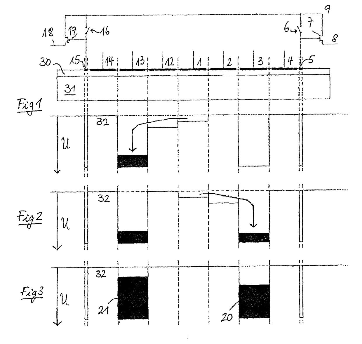
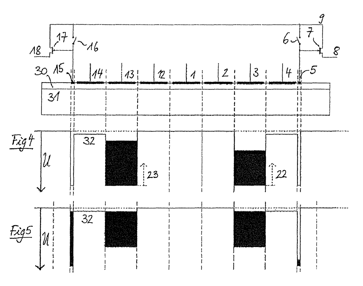
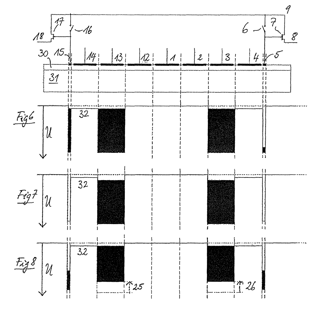
[0029]FIG. 1 shows a cross-sectional schematic of a pixel of a time-of flight imager, with a light-sensitive middle gate 1, a right light-sensitive gate 2, a right integration gate 3, a right output gate 4, a right sense node 5, a right reset switch 6, a right source follower 7, a right output 8, and a left light-sensitive gate 12, a left integration gate 13, a left output gate 14, a left sense node 15, a left reset switch 16, a left source follower 17, and a left output 18. Reference numeral 9 designates the positive supply voltage, 30 the gate oxide. The bulk material 31 is preferably p-doped.

[0030]FIG. 1 also shows a first potential distribution 32 inside the pixel, which is created by applying the appropriate voltages to the gates 1, 2, 3, 4, 5, 12, 13, 14, 15. U designates the voltage axis. The potential distribution in FIG. 1 is such that the electrons, which are generated by the light falling on the light-sensitive gates 1, 2 and 12 are deviated to the left and are collected ...


PUM


Abstract

A time-of-flight imager pixel has a light-sensitive region, a first and a second integration gate associated with the light-sensitive region, a first and a second sense node, a first output gate arranged between the first integration gate and the first sense node and a second output gate arranged between the second integration gate and the second sense node, a method for operating such a pixel includesexposing the light-sensitive region to light so as to optically generate charge carriers;collecting the charge carriers alternatively under the first and second integration gates;adjusting voltages of the first and second output gates and the first and second integration gates, thereby transferring a first portion of the charge carriers from the first integration gate into the first sense node and a second portion from the second integration gate into the second sense node;calculating time-of-flight information based on the first and second portions of charge carriers.adjusting at least one voltage so as to transfer, if respectively the first and / or second integration gate is close to or in saturation, an amount of charge carriers form the first and / or second integration gate into the first and / or second sense node; andtesting whether a voltage change exceeding a given threshold was thereby provoked in the first and / or second sense node.

Description

TECHNICAL FIELD OF THE INVENTION[0001]The present invention generally relates to time-of-flight imaging, more particularly to a method for operating a time-of-flight imager pixel.BRIEF DISCUSSION OF RELATED ART[0002]Time-of-flight distance measuring or imaging systems use active illumination of the scene with a modulated light source. The pixels of a time-of-flight imager are synchronised with the modulated light source and accumulate charges under different integration gates within a period of the modulation. Charges are collected under each integration gate during a different time interval. Depending on the pixel configuration, the time interval can be distinct or partially overlapping. The relative phase difference between the pixel clock and the detected modulated light can be determined from the charge distribution under the integration gates.[0003]In an advantageous method for reading out a time-of-flight imager pixel, only a small portion of the accumulated charge is taken in...

Claims


Application Information

Patent Timeline
Patent Type & Authority Patents(United States)
IPC IPC(8): G01C3/08G01S7/4863G01S17/894
CPCG01S7/481G01S7/4863G01S17/89G01S17/894
Inventor LAMESCH, LAURENTLANDWEHR, JOCHEN
Owner IEE INT ELECTRONICS & ENG SA
Why Eureka
Try Eureka