Atomic layer deposition apparatus using neutral beam and method of depositing atomic layer using the same

a technology of atomic layer and neutral beam, which is applied in the direction of vacuum evaporation coating, electric/magnetic/electromagnetic heating, coating, etc., can solve the problems of physical and electrical damage to a specific material layer or a specific material layer on the semiconductor substrate, atomic bonds of the surface layer are damaged, and dangle bonds

Active Publication Date: 2011-04-05
RES & BUSINESS FOUND SUNGKYUNKWAN UNIV
View PDF2 Cites 288 Cited by
  • Summary
  • Abstract
  • Description
  • Claims
  • Application Information

AI Technical Summary

Benefits of technology

[0014]The present invention also provides a method of depositing an atomic layer without charging a second reaction gas by plasma ions, i.e., without electrical damage, by ionizing and neutralizing the second reaction gas before radiating it onto a substrate to be treated.

Problems solved by technology

However, such equipment may cause physical and electrical damage to a semiconductor substrate or a specific material layer on the semiconductor substrate, since it involves vast quantities of ions for performing an etching (or deposition) process colliding with the semiconductor substrate or specific material layer with hundreds eV of energy.
In addition, atomic bonds of the surface layer are damaged by the bombardment, thereby becoming dangling bonds.
Such dangling bonds may cause physical or electrical damage to the material, or give rise to charge-up damage of a gate insulating layer or electrical damage by notching of polysilicon due to charging of photoresist.
In addition to such physical and electrical damage, there occurs either surface contamination caused by a chamber material, or surface contamination caused by reaction gases such as C—F polymers generated when using a CF-based reaction gas.
Therefore, since the physical / electrical damage caused by such ions in the nanometer-scale semiconductor devices decreases reliability and productivity of the semiconductor devices, it is required to develop an innovative semiconductor etching (or depositing) apparatus and method that may be applied in the future according to the trend of the high integration of the semiconductor devices and resulting reduction of the design rule.
However, the sputtering method makes it very difficult to obtain uniformity across the entire thin layer.
While CVD has the advantages of excellent step coverage and high yield, a temperature of the thin layer during its formation is very high, and the thickness of the thin layer cannot be controlled to a precision of several Å. In addition, since at least two kinds of reaction gas are simultaneously supplied into a reactor, particles may be generated, which may be a source of contamination.

Method used


Image

  • Atomic layer deposition apparatus using neutral beam and method of depositing atomic layer using the same
  • Atomic layer deposition apparatus using neutral beam and method of depositing atomic layer using the same
  • Atomic layer deposition apparatus using neutral beam and method of depositing atomic layer using the same

Examples


Embodiment Construction

[0024]Hereinafter, exemplary embodiments of the present invention will be described with reference to the accompanying drawings. In the following description and the drawings, the same reference numerals are used to designate the same or similar components, and such components will be described only once.

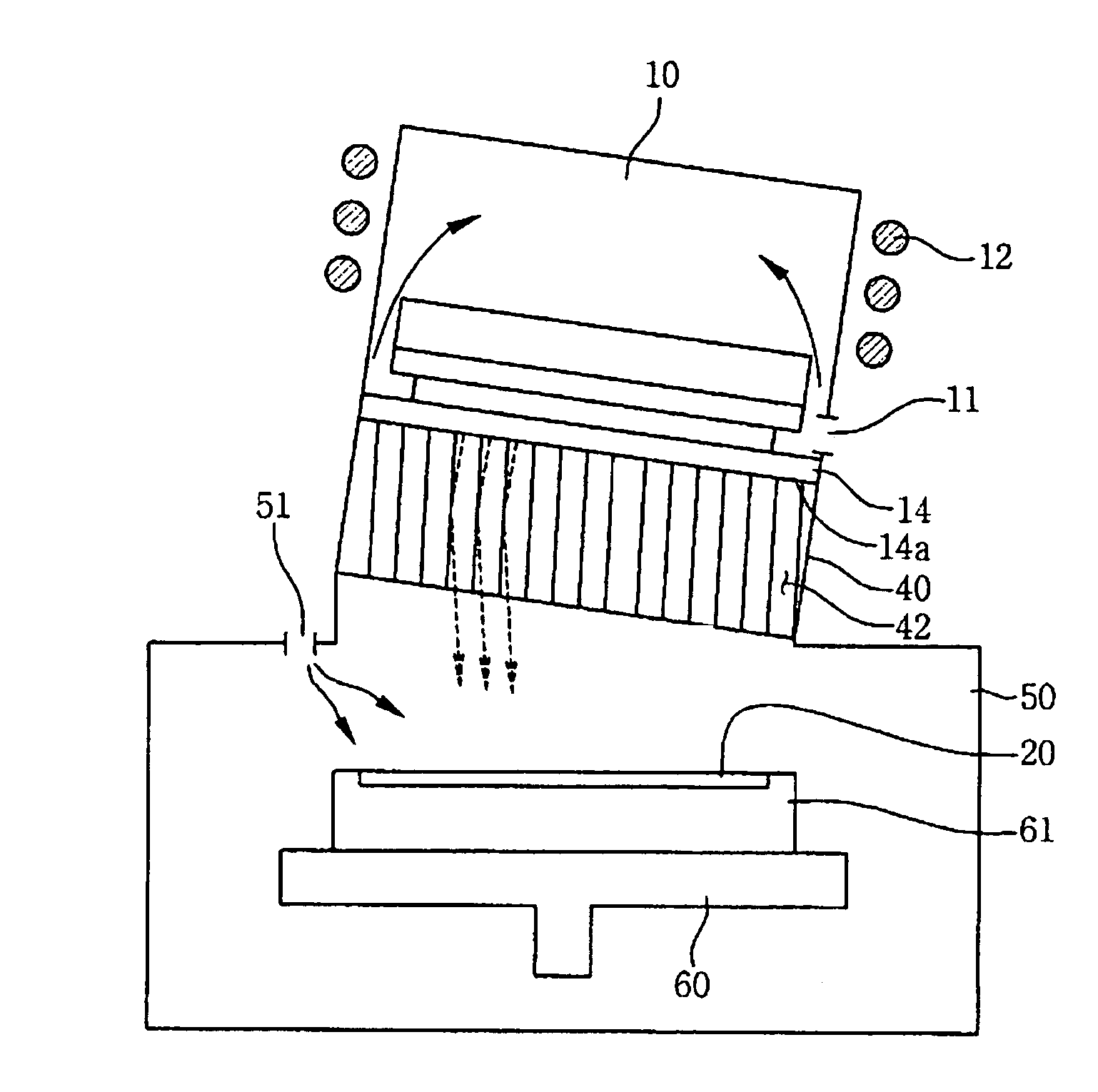
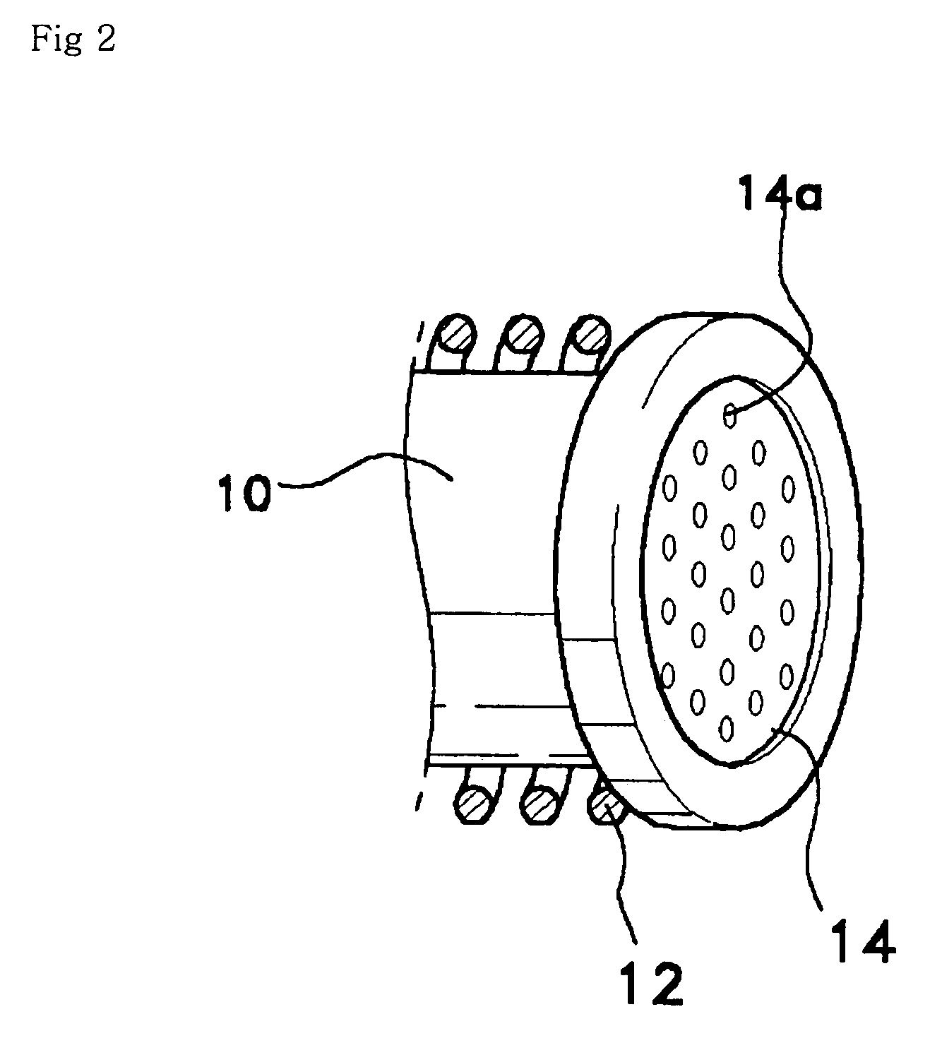
[0025]FIG. 1 is a schematic diagram illustrating an apparatus for depositing an atomic layer using a neutral beam in accordance with an exemplary embodiment of the present invention, FIG. 2 is a perspective view illustrating an ion source and a grid shown in FIG. 1, and FIG. 3 is a perspective view illustrating a reflective body shown in FIG. 1.

[0026]One aspect of the present invention provides more preferable conditions than the ALD process of a nanometer-scale semiconductor device on the theoretical basis of a neutral beam, which will be described with reference to FIGS. 1 to 3.

[0027]In FIG. 1, an ion beam generated from an ion source 10 passes through a plurality of grid holes 14...


PUM

PropertyMeasurementUnit
incident angleaaaaaaaaaa
reflection angleaaaaaaaaaa
pressureaaaaaaaaaa

Abstract

Disclosed are an atomic layer deposition apparatus using a neutral beam and a method of depositing an atomic layer using the apparatus, capable of converting an ion beam into a neutral beam and radiating it onto a substrate to be treated. The method uses an apparatus for supplying a first reaction gas containing a material that cannot be chemisorbed onto a substrate to be treated into a reaction chamber in which the substrate is loaded, and forming a first reactant adsorption layer containing a material that cannot be chemisorbed onto the substrate; and radiating a neutral beam generated by the second reaction gas onto the substrate on which the first reactant adsorption layer is formed, and removing a material not chemisorbed onto the substrate from the first reactant adsorption layer to form a second reactant adsorption layer. It is possible to perform a process without damage due to charging with the apparatus for depositing an atomic layer using a neutral beam and the method of depositing an atomic layer using the apparatus.

Description

BACKGROUND OF THE INVENTION[0001]1. Field of the Invention[0002]The present invention relates to an atomic layer deposition apparatus using a neutral beam and a method of depositing an atomic layer using the apparatus, and more particularly, to an atomic layer deposition apparatus using a neutral beam and a method of depositing an atomic layer using the apparatus in which a second reaction gas is ionized to form plasma, and a resulting flux of radicals, i.e. an ion beam, is neutralized and radiated onto a substrate to be treated.[0003]2. Description of the Prior Art[0004]Due to increasing demand for highly integrated semiconductor devices, recent years have seen continuous reduction of a semiconductor integrated circuit design rule to the point of a critical dimension not more than 90 nm. Nowadays, in order to implement such nanometer-scale semiconductor devices, ion enhancement equipment such as a high density plasma apparatus, a reactive ion etcher, and so on are being widely used...

Claims


Application Information

Patent Timeline
Patent Type & Authority Patents(United States)
IPC IPC(8): C23C16/00H05B6/00H05B7/00C23C14/28C23C14/30
CPCC23C16/452C23C16/45544C23C16/45536C23C16/4551A47G9/10
Inventor YEOM, GEUN-YOUNGLEE, DO-HAINGPARK, BYOUNG-JAEAHN, KYEONG-JOON
Owner RES & BUSINESS FOUND SUNGKYUNKWAN UNIV
Why Eureka
Try Eureka