Tunable optical active elements

a technology of optical active elements and tunable elements, which is applied in the field of tunable optical active elements, can solve the problems of difficult implementation of expensive mechanical systems, limited tuning range or many expensive production steps, and inability to change the shape of gratings, etc., and achieves large tuning range, low cost, and linear strain in grating period direction.

Inactive Publication Date: 2011-04-05
ETH ZZURICH
View PDF21 Cites 8 Cited by
  • Summary
  • Abstract
  • Description
  • Claims
  • Application Information

AI Technical Summary

Benefits of technology

[0021]A further need in optics consists in optical elements which easily allow to shift the phase of e.g. a light beam. When light travels through a medium, its wavelength decreases inversely proportional to the refractive index of the medium λ=λ0 / n, wherein λ represents the wavelength of light in the medium, λ0 is the wavelength of the light in vacuum and n denotes the refractive index of the medium. When light travels a distance of l through a medium with refractive index n, a phase retardation of φ=2π(n−1)l / λ is introduced compared to a beam traveling in vacuum. If the thickness of the medium is changed by a value of Δl, the phase difference between the two beams changes by Δφ=2π(n−1)Δl / λ. As it will become obvious from the subsequent explanations the herein disclosed invention provides a method and a device which allow to shift the phase of light in an easy and cost efficient manner.
[0031]In an embodiment of the invention the actuator and if appropriate the grating are implemented in at least one deformable material. One advantage of such an implementation is a higher linear strain in grating period direction. This has the effect that the grating can achieve a large tuning range (about 150 times higher than any known implementations based on piezo-ceramic actuator materials). Further advantages of the present invention consist in that the manufacturing process is at a very low cost, simple and fast. In difference to previous systems which require several complicated micromachining processes (i.e. comb-drive driven tunable gratings), the production of a preferred embodiment of the invention requires relative inexpensive and commercially available materials such as PDMS (Polydimethylsiloxane, a widely used silicon-based organic polymer), Carbon Black or 3M VHB4910, 3M 9460 Acrylic Elastomers, Elastosil 625 and coating metals such as Au (Gold), Al (Aluminum) or ITO (Indium Tin Oxide), whereas this is only a selection of products.
[0033]Gratings and phase shifters according to the present invention can be miniaturized which is important e.g. to make displays with small pixels or to be used in microscopes. Diffraction gratings have good diffractive properties (wavelength separation) down to 10 lines per diffraction grating. This means that theoretically, a resolution (smallest grating size) of 10×10 μm2 can be achieved. A further advantage is that the mechanical impact is in plane (not as in rotated grating structures).
[0039]It has been shown that in certain fields of application it is advantageous when the polymer film acting as intermediate layer is prestretched by a certain amount, before the deformable grating is attached onto the polymer film and then the polymer film and the deformable grating are stretched again before they are attached to an encompassing holding means and the electrodes are applied. Improved optical efficiency may be obtained in that the polymer film is stretched by 200%, then the deformable grating is applied and the polymer film and the deformable grating are stretch to total 300% before electrodes are applied and the polymer film is attached to the holding means.
[0054]The advantage of changing the grating period and not the angle of the grating is the simple implementation and the fact that the −m and the +m order change their angle equally. This allows among several other applications the use in tunable structured illumination microscopes (described below). Additionally, such systems can be used in inexpensive natural color displays as well as in miniaturized tunable spectrometers or as expander in virtual displays. The tunable transmission grating not only outperforms existing product from the technical point of view but it is also commercially very attractive. The materials used for the production are not only inexpensive but the polymers show also excellent optical properties. Transmittance measurements showed for example that within the wavelength range of 400 nm to 800 nm, less than 1% of the light is absorbed by a 1 mm thick layer. Another major advantage is the simple fabrication process. Depending on the embodiment, two or three production steps are required.

Problems solved by technology

Although some of these gratings are employed in commercially successful products, they are often limited in their tuning range or require many expensive production steps.
These materials make it impossible to change the shape of the gratings.
As state of the art solutions show, the rotation of gratings involves expensive mechanical systems that are difficult to implement in a micro system.
Such devices require either high investments due to complicated production processes or achieve only relatively small tuning ranges.
Due to the function principle both solutions have the disadvantage that it is e.g. not possible to miniaturize them.
One disadvantage is that the grating is based on a fixed pattern of alternating refractive indices.
Due to the fact that this grating relies on the piezo electric effect of the substrate only limited pitch variation is possible and therefore no large tuning range results.
A further difficulty consists in that the making of such a device is relatively expensive.
One problem consists in that the electrodes are arranged lateral to the grating.
Thereby it becomes not possible to miniaturize the device.
However, the lens does not seem to be very accurate.
The above mentioned prior art devices are not only expensive in production but also have the disadvantage of not being practical in the transmission mode.

Method used


Image

  • Tunable optical active elements
  • Tunable optical active elements
  • Tunable optical active elements

Examples


Embodiment Construction

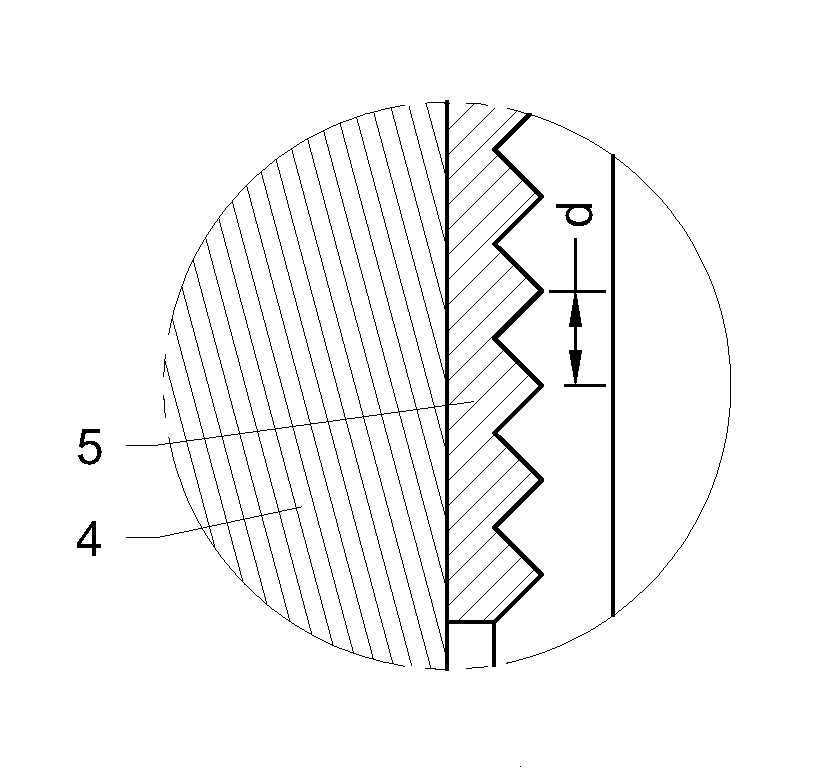
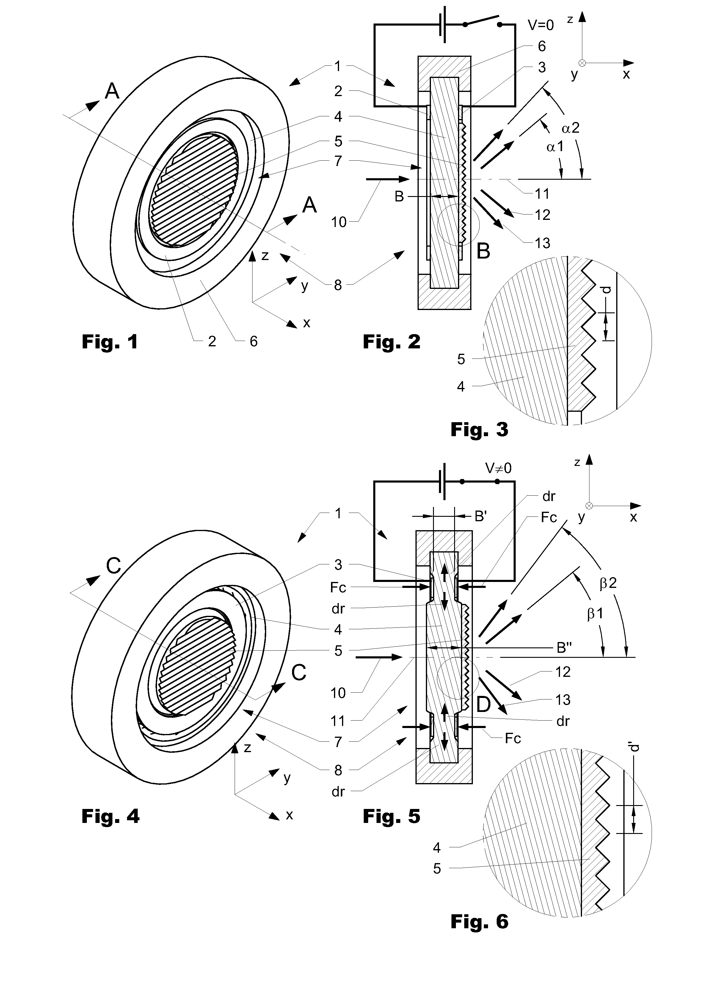
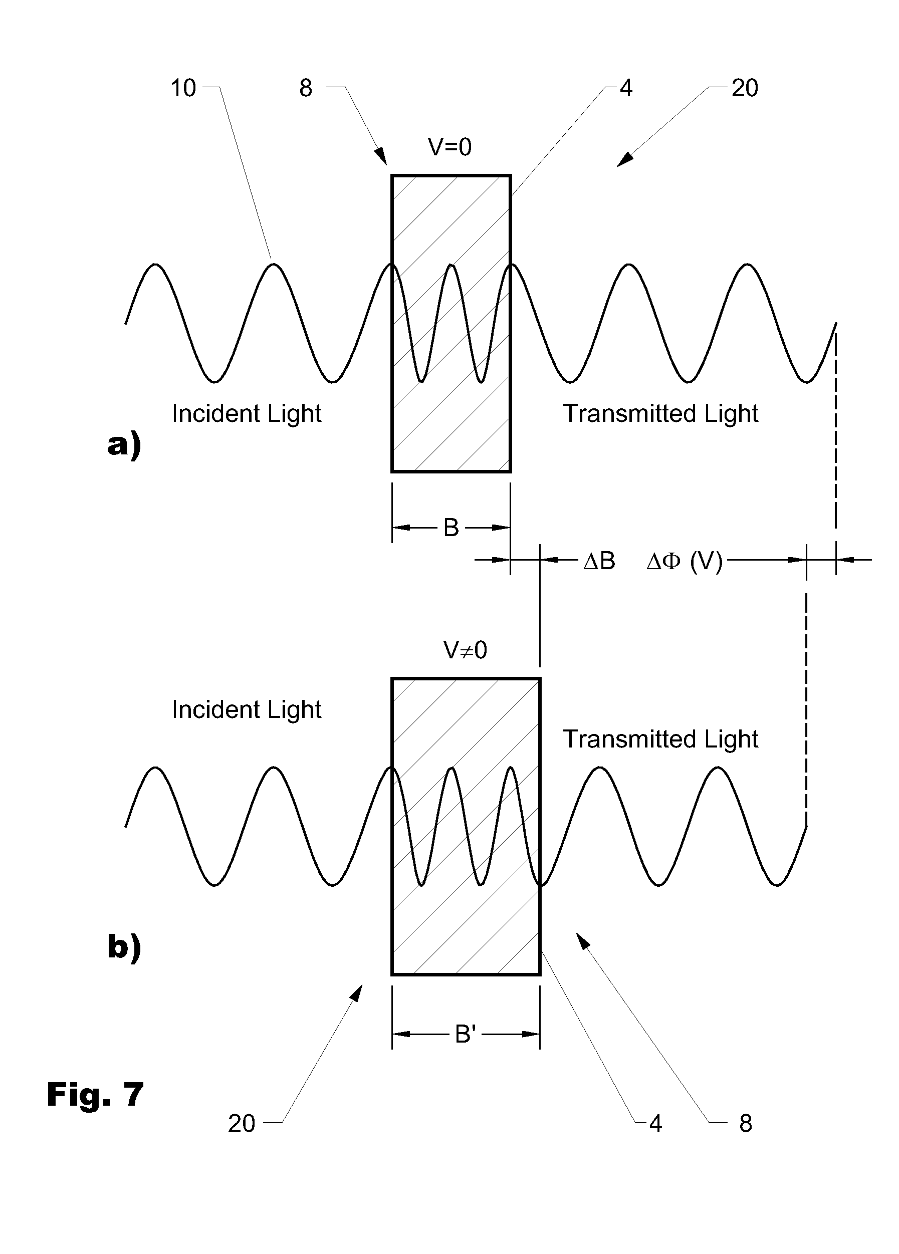
[0091]FIG. 1 through FIG. 6 are schematically showing a first embodiment of an optical element 1 according to the present invention, here a translucent tunable diffraction grating 1. While FIG. 1 is showing the diffraction grating 1 in an undeformed state, FIG. 4 is showing the same diffraction grating 1 in a deformed state. FIG. 2 is showing a cross-section along xz-plane through the centre of the diffraction grating according to FIG. 1 along line AA. FIG. 5 is showing a cross-section along xz-plane through the center of the diffraction grating according to FIG. 4 along line CC. FIG. 3 is showing detail B of FIG. 2 and FIG. 6 is showing detail D of FIG. 5.

[0092]The diffraction grating 1 comprises an upper and a lower electrode 2, 3 which encompass a translucent intermediate layer 4 and an optically active grating area 5. The electrodes 2, 3 act as driving plates of a driving means 15 to locally compress the intermediate layer 4 in a controlled manner. In the herein shown embodiment...


PUM


Abstract

The invention is directed to different optical active elements (1, 20, 22) such as tunable diffraction gratings and tunable phase shifters having in general a similar setup. The optical active elements (1, 20, 22) comprise an intermediate layer (4) made out of a deformable material which is mechanically interconnected to a driving means. The driving means comprises a first and a second driving plate (2, 3) arranged in general opposite to each other on opposite sides of and at least partially covering the intermediate layer (4) such that a local compression of the intermediate layer (4) by the driving plates (2, 3) causes a local reduction of the thickness in a first direction. This reduction in a first direction causes a secondary deformation of the intermediate layer in a second direction which results in a change of the optical behavior of the optical active element.

Description

FIELD OF THE INVENTION[0001]The invention lies in the field of tunable optical active elements such as phase shifters and transmission gratings, e.g. for adaptive optics and microscopy.BACKGROUND OF THE INVENTION[0002]A diffraction grating is an optical element that consists of a reflecting or transparent substrate whose surface contains fine grooves or rulings that are equally spaced. When light is incident on a diffraction grating, diffractive and mutual interference effects occur and light is reflected or transmitted in discrete directions called orders. Because of their dispersive properties, gratings are commonly used in monochromators and spectrometers. These devices were first manufactured by German physicist Joseph von Fraunhofer in 1821.[0003]Diffraction gratings have been a research topic for many decades. At the beginning, the design and the functional principle of the gratings were of major interest. In recent years, tunable diffraction gratings became popular, which all...

Claims


Application Information

Patent Timeline
Patent Type & Authority Patents(United States)
IPC IPC(8): G02B1/06
CPCG02B5/1828G02B5/1847G02B26/0808G02B5/18G02B26/06
Inventor ASCHWANDEN, MANUELBECK, MARKUS DANIELBELYAEV, YURYSTEMMER, ANDREAS
Owner ETH ZZURICH
Why Eureka
Try Eureka