Interferometer device and method

a technology of interferometer and interferometer, which is applied in the direction of instruments, radiation measurement, x-ray spectral distribution measurement, etc., can solve the problems of time-consuming tomography scans, higher expended dose, and difficult fabrication process of gratings

Inactive Publication Date: 2011-04-12
CSEM CENT SUISSE DELECTRONIQUE & DE MICROTECHNIQUE SA RECH & DEV
View PDF11 Cites 78 Cited by
  • Summary
  • Abstract
  • Description
  • Claims
  • Application Information

AI Technical Summary

Problems solved by technology

Generally, an increase in the periodicity and / or structure depth of gratings renders the fabrication process of the gratings more difficult.
However, compared to dual X-ray imaging, tomography scans may be time consuming, and the expended dose may be higher.

Method used


Image

  • Interferometer device and method
  • Interferometer device and method
  • Interferometer device and method

Examples


Embodiment Construction

Summary of Embodiments of the Invention

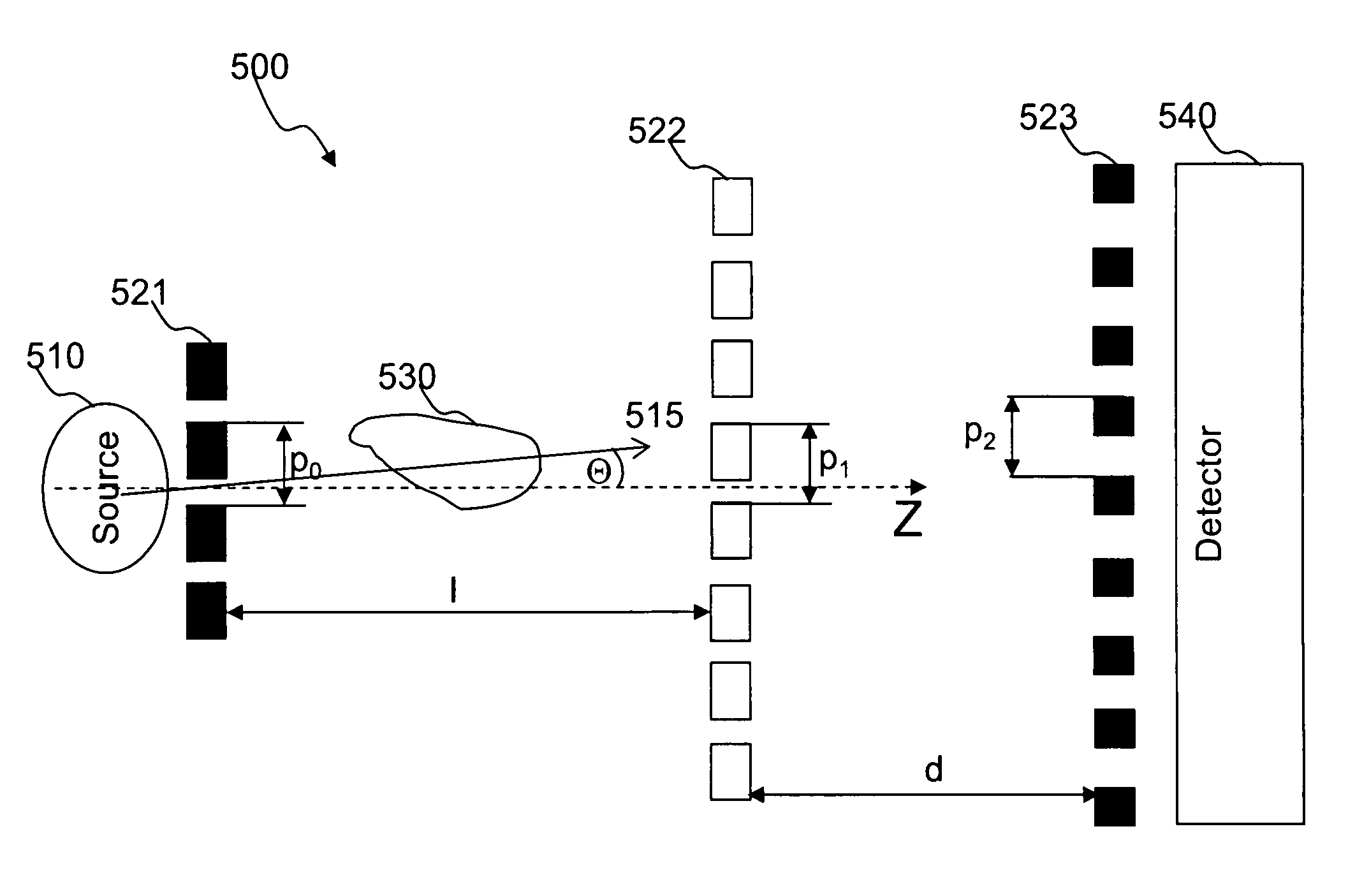
[0036]Embodiments of the invention disclose an interferometer device comprising an electromagnetic radiation source emitting radiation; a phase grating having a first aspect ratio; an absorption grating having a second aspect ratio; and a detector. The electromagnetic radiation source, the phase grating, the absorption grating and the detector are radiatively coupled with each other. The absorption grating is positioned between the detector and the phase grating; the electromagnetic radiation source is positioned in front of the source grating; and the phase grating is designed such to cause on at least one wavelength of radiation passing through the grating bars a phase shift (Δφ) of less than π relative to radiation passing between the grating bars with respect to the at least one wavelength.

[0037]In embodiments, the phase grating is designed such to cause one of the following phase shifts: π / 2, π / 4. In embodiments, the electromagnetic radiat...


PUM


Abstract

The present invention discloses an interferometer device and method. In embodiments, the device comprises an electromagnetic radiation source emitting radiation having a first mean wavelength λLE; a phase grating having a first aspect ratio; an absorption grating having a second aspect ratio; and a detector. The electromagnetic radiation source, the phase grating, the absorption grating and the detector are radiatively coupled with each other. The absorption grating is positioned between the detector and the phase grating; the electromagnetic radiation source is positioned in front of the source grating; and wherein the phase grating is designed such to cause a phase shift that is smaller than π on the emitted radiation. Additional and alternative embodiments are specified and claimed.

Description

CROSS-REFERENCE TO RELATED APPLICATIONS[0001]This patent application claims priority from U.S. Provisional Patent Application No. 60 / 988,278 filed on Nov. 15, 2007, the disclosure of which is incorporated herein by reference in its entirety.FIELD OF THE INVENTION[0002]This invention relates to imaging devices and methods, and more particularly, to imaging devices and methods accomplished with interferometers.BRIEF DESCRIPTION OF THE DRAWINGS[0003]These and further features and advantages of the invention will become more clearly understood in the light of the ensuing description of embodiments thereof, given by way of example only, with reference to the accompanying figures, wherein:[0004]FIG. 1A is a schematic illustration of a setup of an interferometer device;[0005]FIG. 1B is a schematic illustration of a grating;[0006]FIG. 2A is a schematic illustration of amplitude interference patterns for a phase grating designed to cause a phase shift of Δφ<π / 2, according to an embodiment...

Claims


Application Information

Patent Timeline
Patent Type & Authority Patents(United States)
IPC IPC(8): G03H5/00G01T1/36
CPCG01B15/025G01N23/04G01B9/02024G01B2290/30G21K2207/005G01N23/041
Inventor KOTTLER, CHRISTIANKAUFMANN, ROLF
Owner CSEM CENT SUISSE DELECTRONIQUE & DE MICROTECHNIQUE SA RECH & DEV
Why Eureka
Try Eureka