Profile of flash memory cells

a flash memory and profile technology, applied in the direction of semiconductor devices, electrical devices, transistors, etc., can solve the problems of memory failure and increase the likelihood of shortening floating gates, and achieve the effect of reducing the likelihood of floating gate shortening and improving the erase performance of the resultant flash memory

Inactive Publication Date: 2011-04-19
TAIWAN SEMICON MFG CO LTD
View PDF15 Cites 7 Cited by
  • Summary
  • Abstract
  • Description
  • Claims
  • Application Information

AI Technical Summary

Benefits of technology

[0011]The advantageous features of the present invention include improved erase performance of the resulting flash memory, and reduced likelihood of floating gate shorting.

Problems solved by technology

As a result, the resulting memory fails.
Accordingly, the likelihood of having shorted floating gates increases.

Method used


Image

  • Profile of flash memory cells
  • Profile of flash memory cells
  • Profile of flash memory cells

Examples


Embodiment Construction

[0016]The making and using of the presently preferred embodiments are discussed in detail below. It should be appreciated, however, that the present invention provides many applicable inventive concepts that can be embodied in a wide variety of specific contexts. The specific embodiments discussed are merely illustrative of specific ways to make and use the invention, and do not limit the scope of the invention.

[0017]A novel flash memory structure and the method of forming the same are provided. The intermediate stages of manufacturing a preferred embodiment of the present invention are illustrated. Throughout the various views and illustrative embodiments of the present invention, like reference numbers are used to designate like elements.

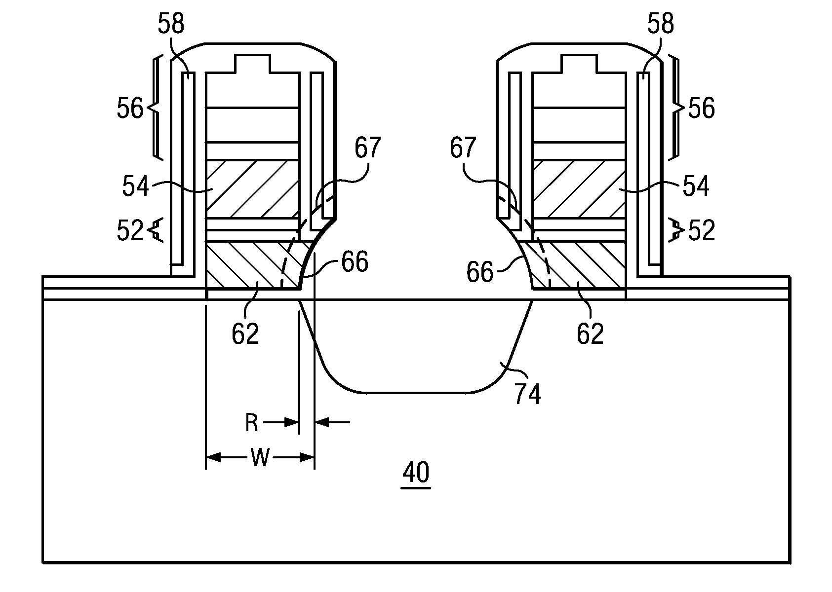
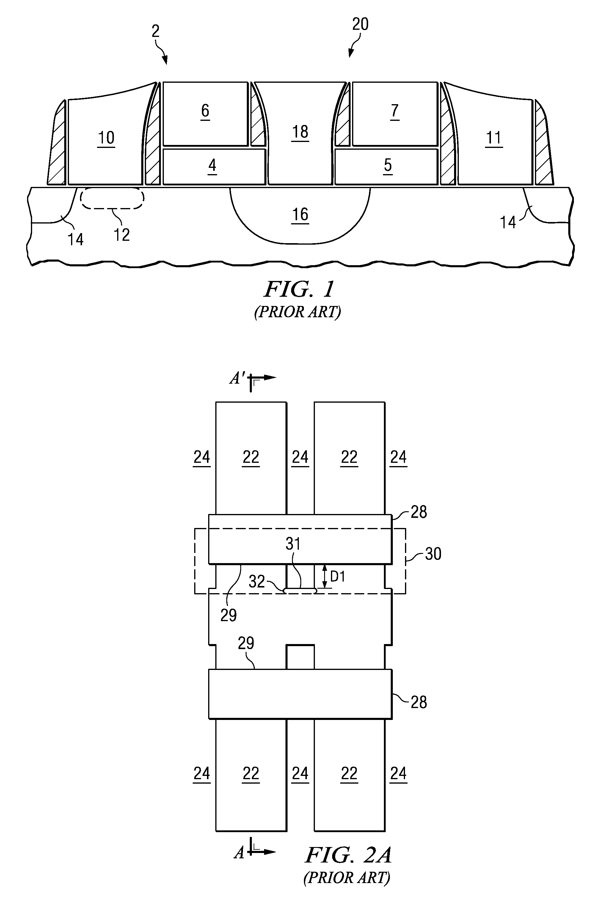
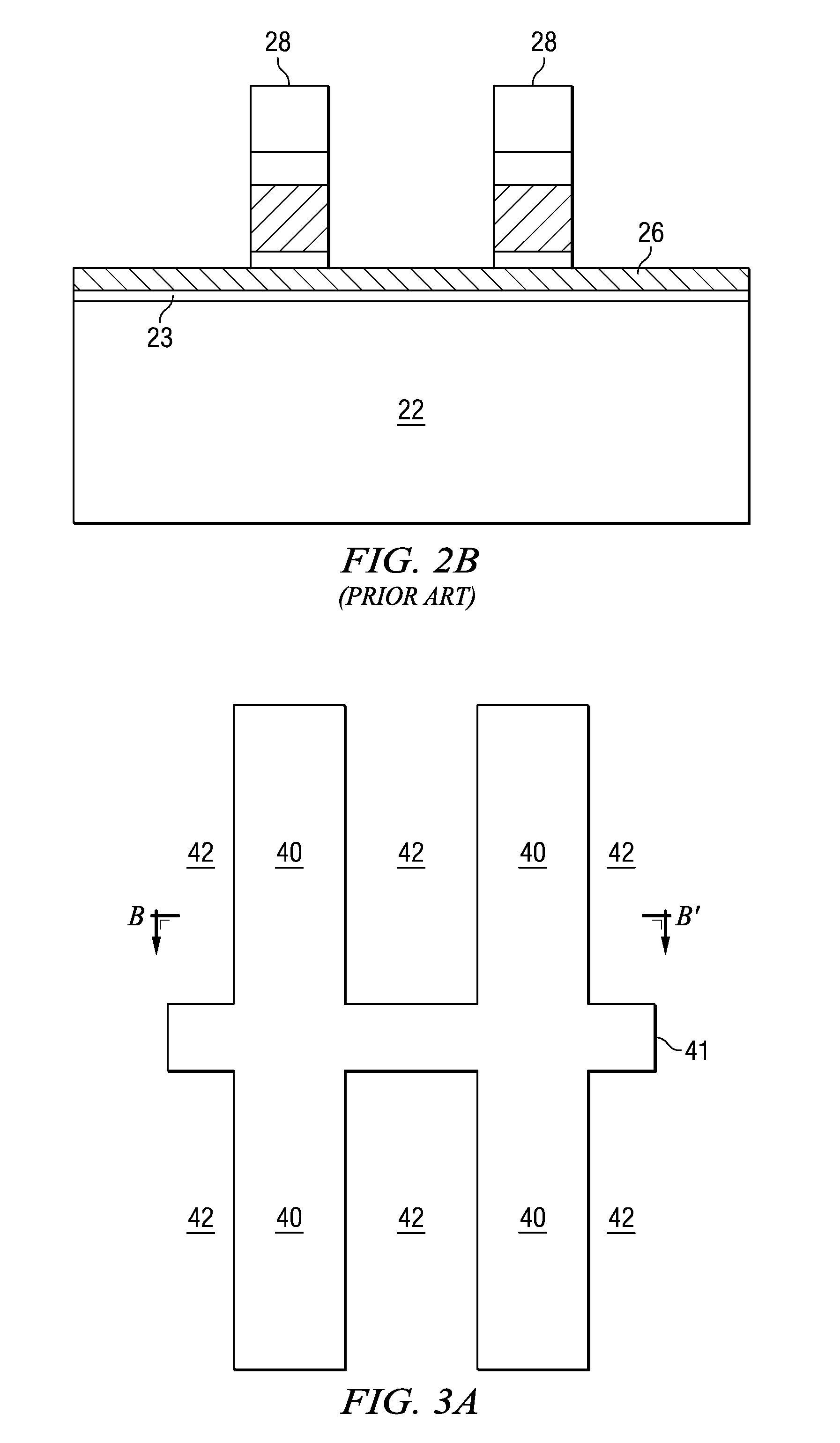
[0018]FIGS. 3A and 3B illustrate a starting structure of an embodiment of the present invention. FIG. 3A is a top view of a portion of semiconductor substrate 38 (refer to FIG. 3B), which includes active region 40 defined by shallow trench isolati...


PUM


Abstract

A semiconductor structure includes a semiconductor substrate; a tunneling layer on the semiconductor substrate; a source region adjacent the tunneling layer; and a floating gate on the tunneling layer. The floating gate comprises a first edge having an upper portion and a lower portion, wherein the lower portion is recessed from the upper portion. The semiconductor structure further includes a blocking layer on the floating gate, wherein the blocking layer has a first edge facing a same direction as the first edge of the floating gate.

Description

TECHNICAL FIELD[0001]This invention relates generally to semiconductor devices, and more particularly to the structure and manufacturing methods of flash memory cells.BACKGROUND[0002]Flash memories have become increasingly popular in recent years. A typical flash memory comprises a memory array having a large number of memory cells arranged in blocks. Each of the memory cells is fabricated as a field-effect transistor having a control gate and a floating gate. The floating gate is capable of holding charges and is separated from source and drain regions contained in a substrate by a layer of thin oxide. Each of the memory cells can be electrically charged by injecting electrons from the substrate through the oxide layer onto the floating gate. The charges can be removed from the floating gate by tunneling the electrons to the source region or an erase gate during an erase operation. The data in flash memory cells are thus determined by the presence or absence of charges in the float...

Claims


Application Information

Patent Timeline
Patent Type & Authority Patents(United States)
IPC IPC(8): H01L29/788
CPCH01L21/28273H01L27/115H01L29/7881H01L27/11521H01L29/42328H01L27/11519H01L29/40114H10B69/00H10B41/10H10B41/30
Inventor LIU, SHIH-CHANGCHANG, CHU-WEILO, CHI-HSINTSAI, CHIA-SHIUNG
Owner TAIWAN SEMICON MFG CO LTD
Why Eureka
Try Eureka