Nonvolatile memory device and method of fabricating the same comprising a dual fin structure

a non-volatile memory and fin structure technology, applied in the direction of semiconductor devices, electrical devices, transistors, etc., can solve the problems of difficult manufacturing process of fin-fets, difficulty in forming bit line contact with low resistance, and large distance between fins, so as to achieve more economical fabrication of non-volatile memory devices, lower bit line contact resistance, and high integration

Inactive Publication Date: 2011-04-26
SAMSUNG ELECTRONICS CO LTD
View PDF13 Cites 10 Cited by
  • Summary
  • Abstract
  • Description
  • Claims
  • Application Information

AI Technical Summary

Benefits of technology

[0008]Example embodiments provide a nonvolatile memory device having higher integration and lower bit line contact resistance. Example embodiments also provide a method of more economically fabricating the nonvolatile memory device.

Problems solved by technology

However, it may be difficult to form a bit line contact with low resistance in the cases of a fin-FET and a fin memory cell, and a fin-FET including a fin formed on an insulating layer.
In addition, because the fins are structurally bent to form the bit line contacts, the process of manufacturing the fin-FET may be more difficult.
However, the distance between the fins may become larger due to the source and drain regions, and as a result, the integration density of the fin-FET may be lower.

Method used


Image

  • Nonvolatile memory device and method of fabricating the same comprising a dual fin structure
  • Nonvolatile memory device and method of fabricating the same comprising a dual fin structure
  • Nonvolatile memory device and method of fabricating the same comprising a dual fin structure

Examples


Embodiment Construction

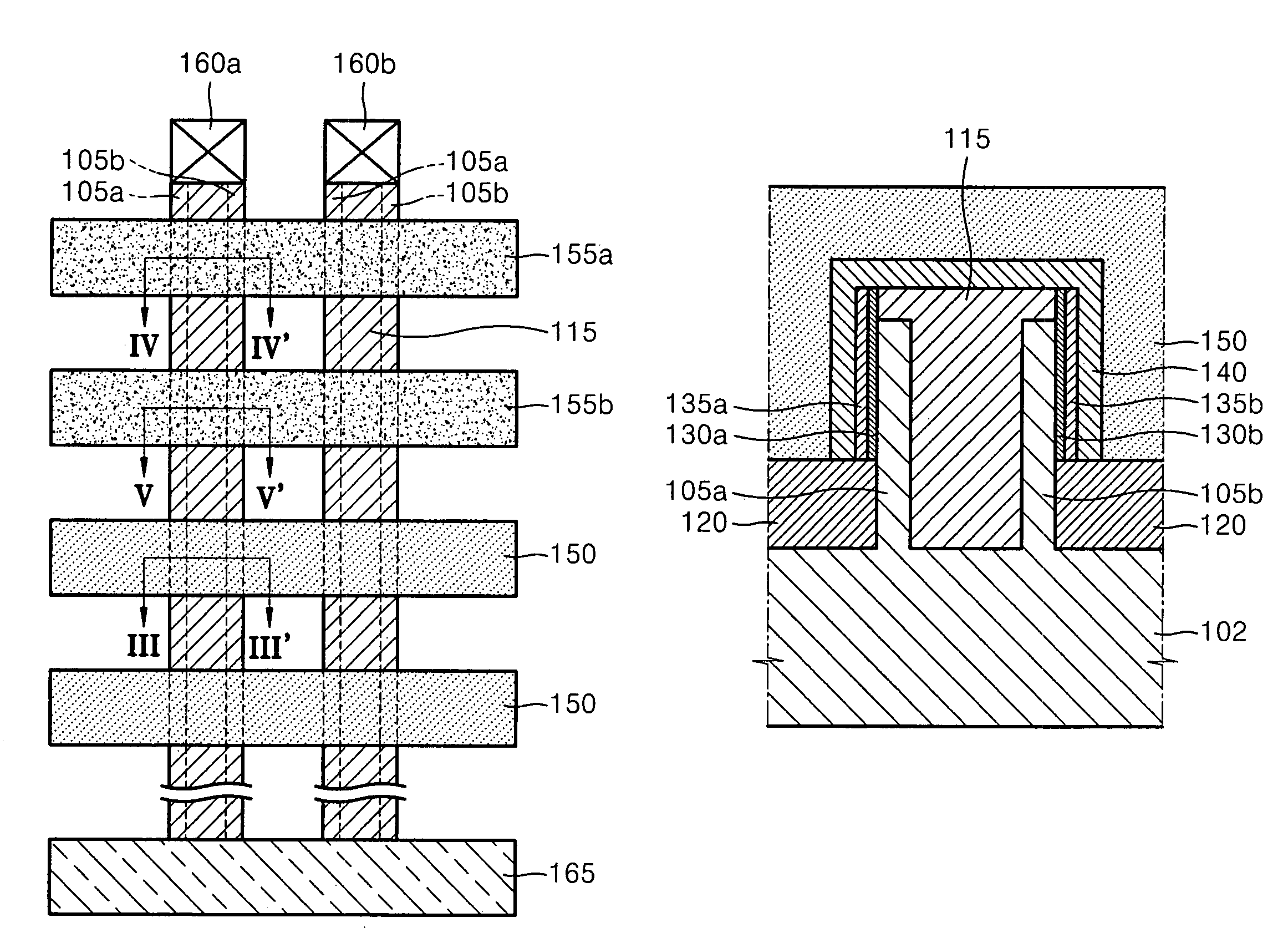
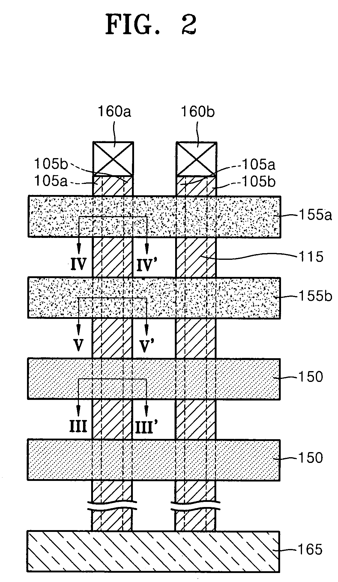
[0026]Reference will now be made in detail to example embodiments, examples of which are illustrated in the accompanying drawings. However, example embodiments are not limited to the embodiments illustrated hereinafter, and the embodiments herein are rather introduced to provide easy and complete understanding of the scope and spirit of example embodiments. In the drawings, the thicknesses of layers and regions are exaggerated for clarity.

[0027]It will be understood that when an element or layer is referred to as being “on,”“connected to” or “coupled to” another element or layer, it may be directly on, connected or coupled to the other element or layer or intervening elements or layers may be present. In contrast, when an element is referred to as being “directly on,”“directly connected to” or “directly coupled to” another element or layer, there are no intervening elements or layers present. Like reference numerals refer to like elements throughout. As used herein, the term “and / or...


PUM


Abstract

A nonvolatile memory device is provided. In the nonvolatile memory device, a semiconductor substrate of a first conductivity type includes first and second fins. A common bit line electrode connects one end of the first fin to one end of the second fin. Control gate electrodes cover the first and second fins and expand across the top surface of each of the first and second fins. A first string selection gate electrode positioned between the common bit line electrode and the control gate electrodes may cover the first and second fins and expand across the top surface of each of the first and second fins. A second string selection gate electrode positioned between the first string selection gate electrode and the control gate electrodes may cover the first and second fins and expand across the top surface of each of the first and second fins.

Description

PRIORITY STATEMENT[0001]This application claims priority under 35 U.S.C. §119 to Korean Patent Application Nos. 2006-0136836 and 2007-0094901, filed on Dec. 28, 2006 and Sep. 18, 2007, respectively, in the Korean Intellectual Property Office (KIPO), the entire contents of which are herein incorporated.BACKGROUND[0002]1. Field[0003]Example embodiments relate to a semiconductor device that stores data via a charge storage layer, and a method of fabricating the same.[0004]2. Description of Related Art[0005]Today, semiconductor devices are required to be both smaller in size and capable of processing large amounts of data at higher operating speeds. Accordingly, much research has been conducted to increase the operating speed and integration density of nonvolatile memory devices used in semiconductor devices. For example, the area of the channel of a Fin-FET semiconductor device can be broadened to enhance the operating speed, and simultaneously the width of the fin of the device can be...

Claims


Application Information

Patent Timeline
Patent Type & Authority Patents(United States)
IPC IPC(8): H01L27/108H01L29/94
CPCH01L27/115H01L27/11521H01L29/66803H01L27/11568H01L29/42336H01L27/11524H10B41/35H10B43/30H10B69/00H10B41/30
Inventor KIM, WON-JOOPARK, YOON-DONGKOO, JUNE-MOKIM, SUK-PILBYUN, SUNG-JAE
Owner SAMSUNG ELECTRONICS CO LTD
Why Eureka
Try Eureka