Semiconductor device having high frequency wiring and dummy metal layer at multilayer wiring structure

a technology of high frequency wiring and multi-layer wiring structure, which is applied in the direction of semiconductor devices, semiconductor/solid-state device details, diodes, etc., can solve the problems of increased parasitic capacity components of inductor and transformer, ineffective prevention of erosion, etc., and achieve the effect of improving the characteristics of semiconductor devices and preventing erosion and dishing

Active Publication Date: 2011-04-26
RENESAS ELECTRONICS CORP
View PDF8 Cites 22 Cited by
  • Summary
  • Abstract
  • Description
  • Claims
  • Application Information

AI Technical Summary

Benefits of technology

[0013]If the configuration as described above is taken, then the number of dummy metals disposed between the high frequency wiring and the semiconductor substrate can be reduced in the region near the high frequency wiring at a top view. As a result, the capacitance (parasitic capacity) between the high frequency wiring and the semiconductor substrate can be suppressed, thereby the characteristics of the high frequency wirings of the inductor and the transformer can be kept favorably. On the other hand, even in the region near the high frequency wiring, because dummy metals are disposed dispersedly therein, erosion and dishing can be prevented effectively, thereby manufacturing the semiconductor devices stably.
[0015]According to the aspect of the present invention, erosion and dishing can be prevented effectively when manufacturing the semiconductor devices provided with high frequency wirings stably and the influences from the surrounding dummy metals on each high frequency wiring can be reduced, thereby improving the characteristics of the semiconductor devices.

Problems solved by technology

However, if no dummy metal is disposed just under such an element as an inductor, then variation might occur among formed patterns when recesses are formed in those patterns, thereby erosion, dishing, etc. might not be prevented effectively.
Furthermore, the present inventor et al have also found a problem that if a high frequency wiring is provided for an inductor, transformer, or the like, the parasitic capacity components of the inductor and the transformer increase due to not only the existence of the dummy metals just under the high frequency wiring, but also the existence of its surrounding dummy metals.

Method used


Image

  • Semiconductor device having high frequency wiring and dummy metal layer at multilayer wiring structure
  • Semiconductor device having high frequency wiring and dummy metal layer at multilayer wiring structure
  • Semiconductor device having high frequency wiring and dummy metal layer at multilayer wiring structure

Examples


first exemplary embodiment

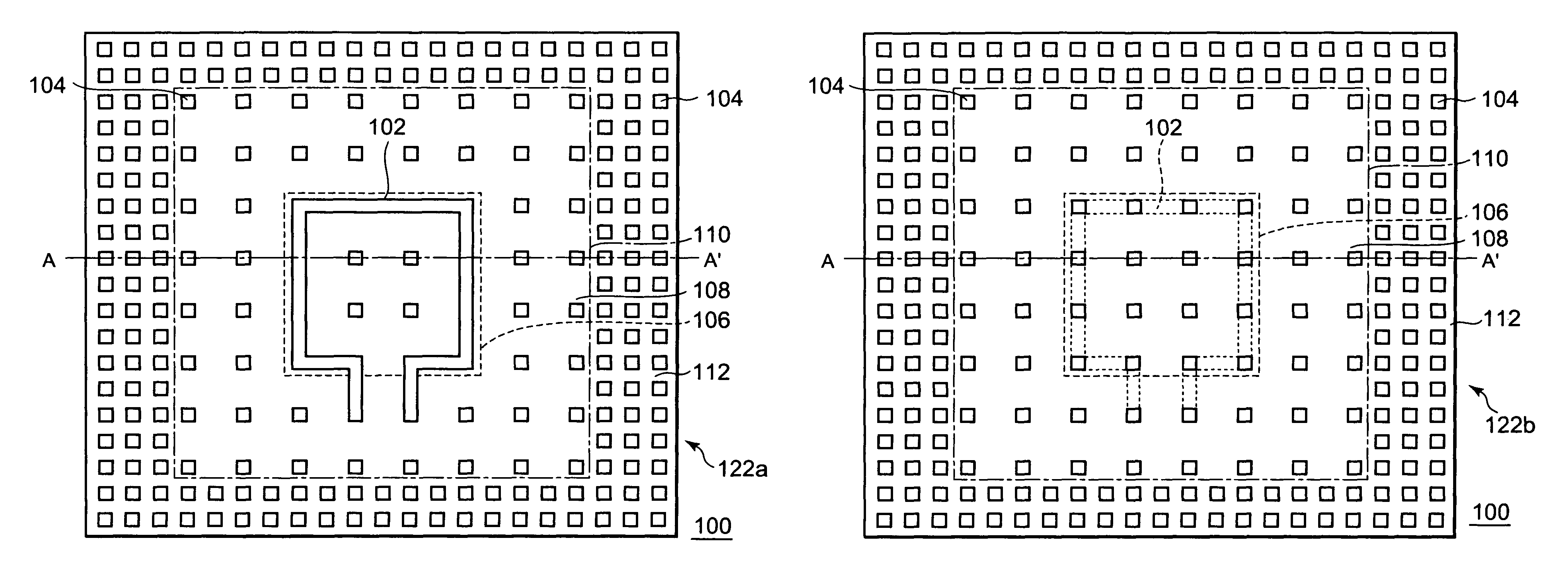
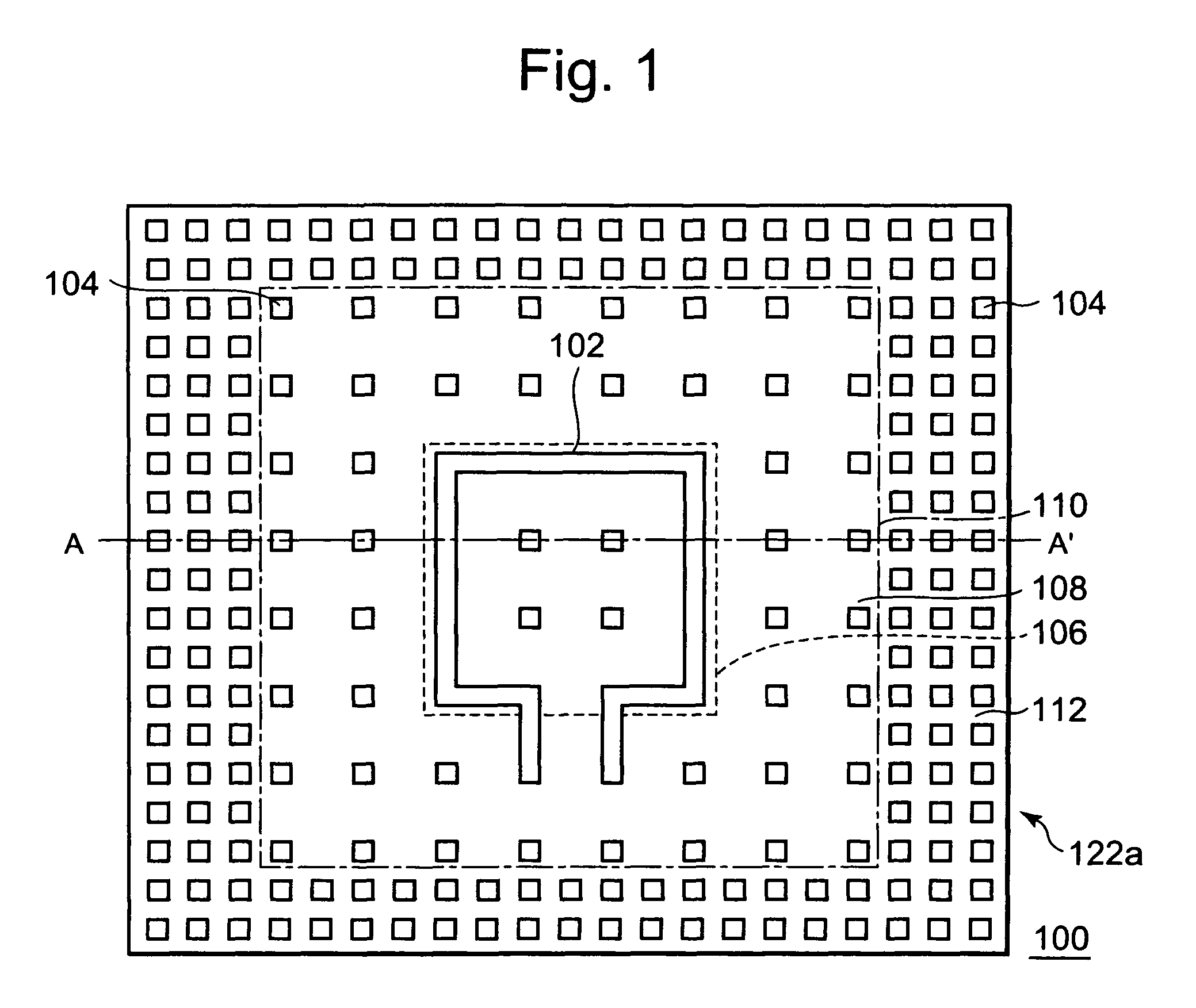
[0025]FIGS. 1 and 2 are top views showing a configuration of a semiconductor device 100 in this first exemplary embodiment respectively. FIG. 3 is a cross sectional view taken on line A-A′ of FIGS. 1 and 2.

[0026]FIG. 1 is a top view of a first wiring layer 122a (first layer) provided with a high frequency wiring 102 and FIG. 2 is a top view of one of second wiring layers 122b (second layer) provided between the first wiring layer 122a and the semiconductor substrate 120. In FIG. 2, a dotted line shows a region superposed on the high frequency wiring 102 at a top view. The high frequency wiring 102 is formed in a coil pattern at a top view and functions as an inductor or transformer. In the high frequency wiring flown a current having a frequency of, for example, 5 GHz or higher. Dummy metals 104 are provided for the first wiring layer 122a and for each of the second wiring layers 122b. A dummy metal means a conductive pattern which substantially does not affect the circuit provided ...

second exemplary embodiment

[0043]In this second exemplary embodiment, a guard ring 116 is provided between a vicinity region 110 surrounding the high frequency wiring 102 and the external region 112. This makes a difference between the semiconductor device in this second embodiment and that 100 in the first embodiment described with reference to FIGS. 1 through 3. The high frequency wiring 102 may be an inductor.

[0044]FIGS. 5 and 6 are top views of the configuration of a semiconductor device 100 in this second exemplary embodiment. FIG. 7 is a cross sectional view taken on line B-B′ of FIG. 6. FIG. 5 is a top view of the first wiring layer 122a (first layer) having the high frequency wiring 102. FIG. 6 is a top view of the second wiring layer 122b (second layer) provided between the first wiring layer 122a and the semiconductor substrate 120.

[0045]As shown in FIG. 7, the guard ring 116 can be formed as a continuous element through all the layers of the multilayer wiring layer 122. Although not limited special...


PUM


Abstract

A semiconductor device includes, a metal wiring, which functions as an inductor or transformer, formed on a first portion of a semiconductor substrate, a plurality of first dummy layers formed in a first density on the first portion of the semiconductor substrate, a plurality of second dummy layers formed in a second density on a second portion of the semiconductor substrate, the second portion surrounding the first portion, and a plurality of third dummy layers formed in a third density higher than the first and second densities on a third portion of the semiconductor substrate, the third portion surrounding the second portion.

Description

BACKGROUND OF THE INVENTION[0001]1. Field of the Invention[0002]The present invention relates to a semiconductor device and more particularly to a semiconductor device that includes a high frequency wiring.[0003]2. Description of Related Art[0004]There is a well-known technique that forms a multilayer wiring structure by forming at first such recesses as wiring grooves, via-holes, etc. in an interlayer insulation film, then by filling the recesses with a metal material and by removing the metal material exposed outside the recesses by a CMP (Chemical Mechanical Polishing) process or the like, thereby forming wirings and via-holes. In case of such a technique, if any density difference exists among those formed wirings and via-holes, then hollows and dents referred to as erosion and dishing often come to appear in the CMP process. And this might result in variation of the in-plane film thickness in the CMP process. In order to prevent the occurrence of such erosion and dishing in the...

Claims


Application Information

Patent Timeline
Patent Type & Authority Patents(United States)
IPC IPC(8): H01L29/00H01L21/8238
CPCH01L23/5227H01L23/585H01L29/86H01L23/645H01L23/66H01L2924/19042H01L2924/30105H01L2924/30107H01L2924/0002H01L2924/00H01L2223/6611H01L23/5283H01L23/528
Inventor UCHIDA, SHINICHI
Owner RENESAS ELECTRONICS CORP
Why Eureka
Try Eureka