Method of manufacturing organic light-emitting device

a technology of light-emitting devices and organic materials, which is applied in the direction of organic semiconductor devices, thermoelectric devices, electroluminescent light sources, etc., can solve the problems of display defect, high probability of existence of display defect in one screen, etc., and achieve high temperature dependence of i-v characteristics, high repair effect, and suppress temperature rise or current rise

Inactive Publication Date: 2011-05-03
JOLED INC
View PDF15 Cites 2 Cited by
  • Summary
  • Abstract
  • Description
  • Claims
  • Application Information

AI Technical Summary

Benefits of technology

[0017]According to the method of manufacturing the organic electroluminescence element of the embodiment of the present invention, at least the element region is put in the atmosphere in which an oxygen concentration is 0.1% or higher and less than 1% and a dew point is −50 degrees or less. Therefore, while suppressing temperature rise or current rise, a pin hole (short-circuit area) in the organic layer causing a display defect is repaired. Thus, the present invention is suitably applied to a large-screen display device using an amorphous silicon TFT in which temperature dependence of the I-V characteristic is high, and a high repairing effect can be obtained.

Problems solved by technology

In the case of applying the organic light-emitting device to a large-screen display device, the probability of existence of a display defect in one screen is very high.
When a display device is turned on and driven, depending on a load of the driving or drive time, a display defect may occur also after completion of manufacture.
The phenomenon appears more conspicuously when the total current amount of the display device increases as the size of the screen increases, and is a very big issue at the time of applying the organic light-emitting device to a large-screen display device.

Method used


Image

  • Method of manufacturing organic light-emitting device
  • Method of manufacturing organic light-emitting device
  • Method of manufacturing organic light-emitting device

Examples


first embodiment

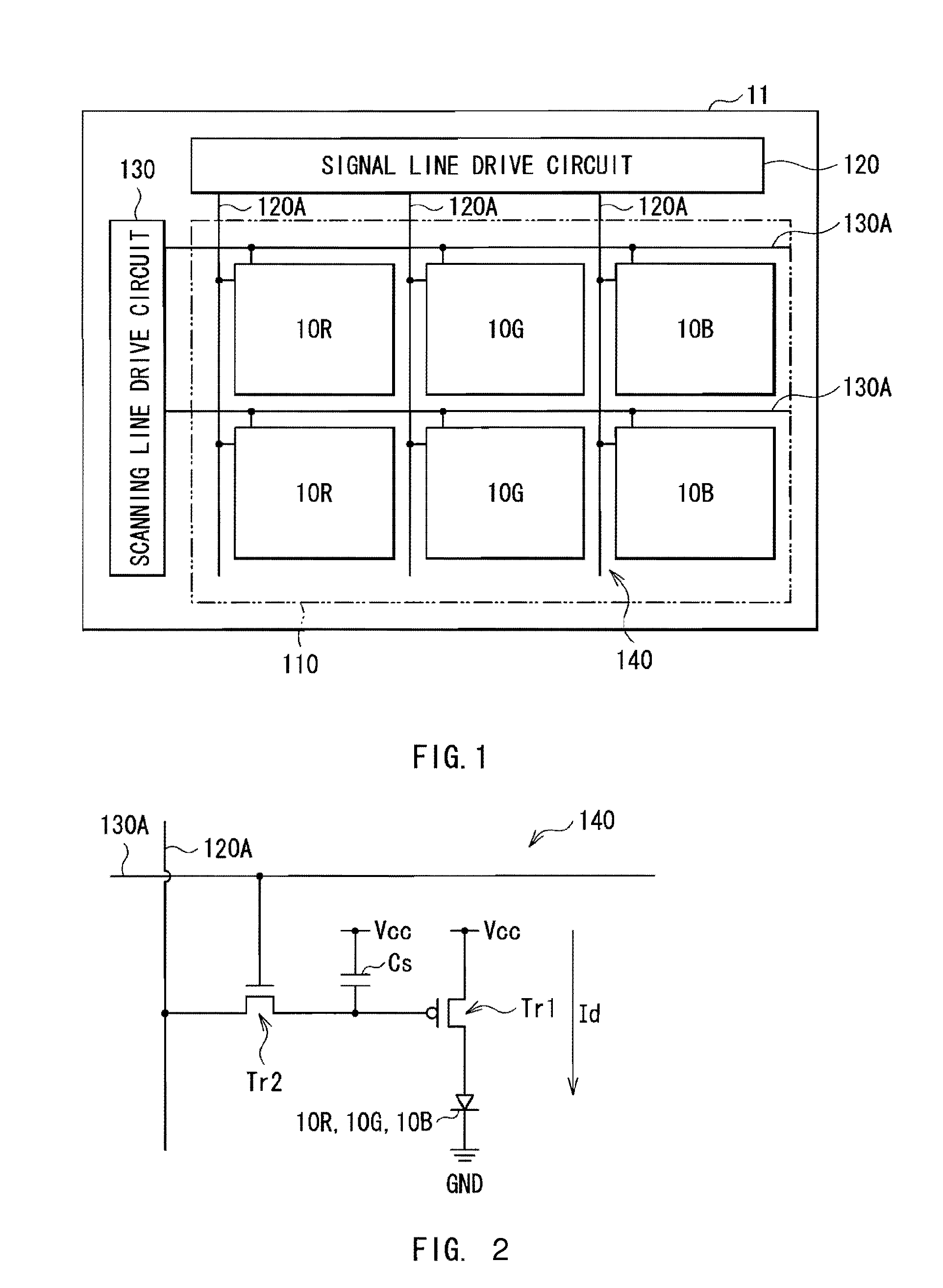
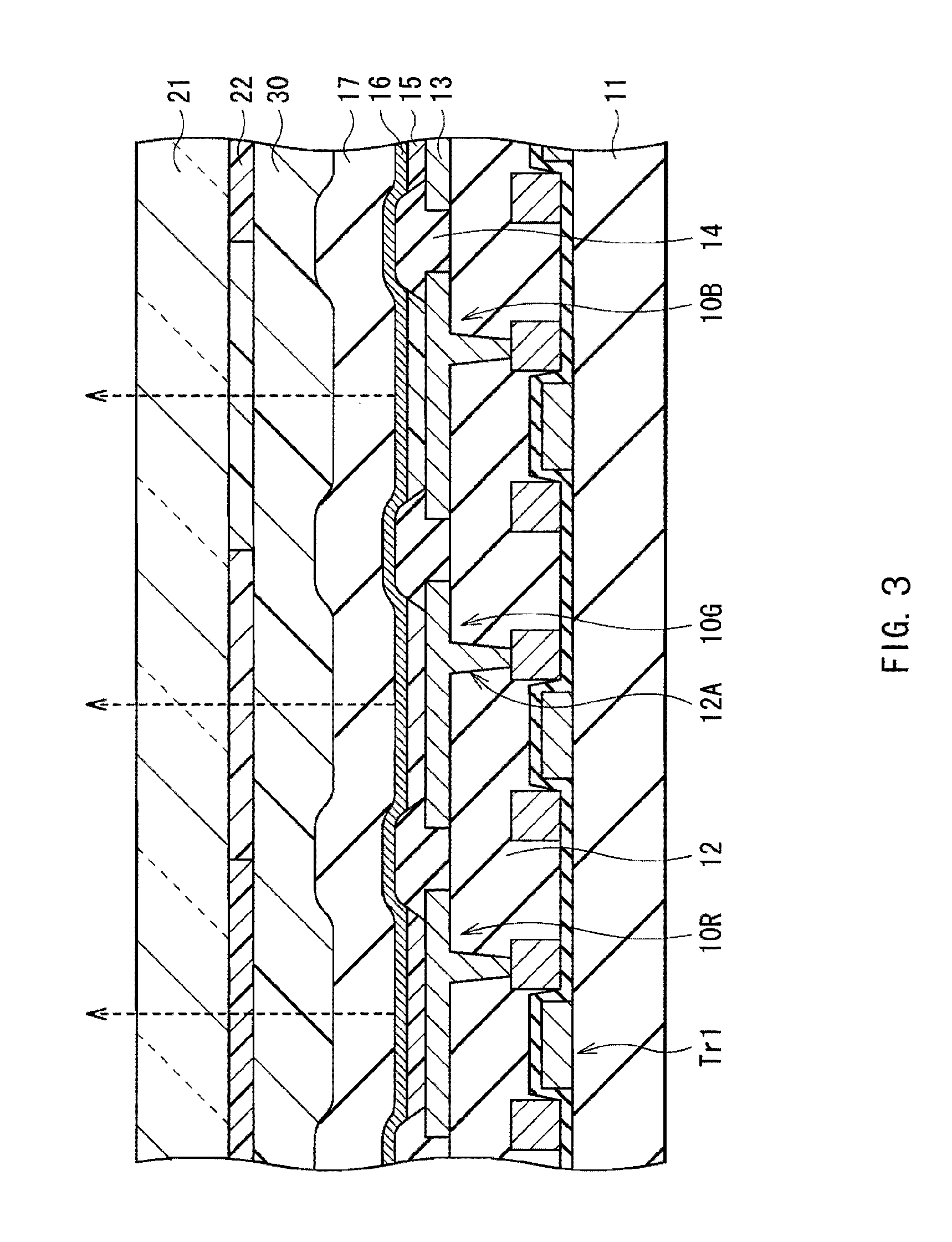
[0039]FIG. 1 shows the configuration of an organic light-emitting device manufactured by a method of manufacturing an organic light-emitting device as a first embodiment of the present invention. The organic light-emitting device is used as an organic EL television and is formed as follows. For example, on a drive substrate 11 made of glass, an element region 110 in which a plurality of organic electroluminescence elements 10R, 10G, and 10B to be described later are disposed in a matrix is formed. A signal line drive circuit 120 and a scanning line drive circuit 130 as drivers for displaying a video image are formed in the peripheries of the element region 110.

[0040]A pixel drive circuit 140 is formed in the element region 110. FIG. 2 shows an example of the pixel drive circuit 140. The pixel drive circuit 140 is an active-type drive circuit having a drive transistor Tr1 and a write transistor Tr2 formed as a layer under an anode 13 which will be described later, a capacitor (holdin...

modification 1

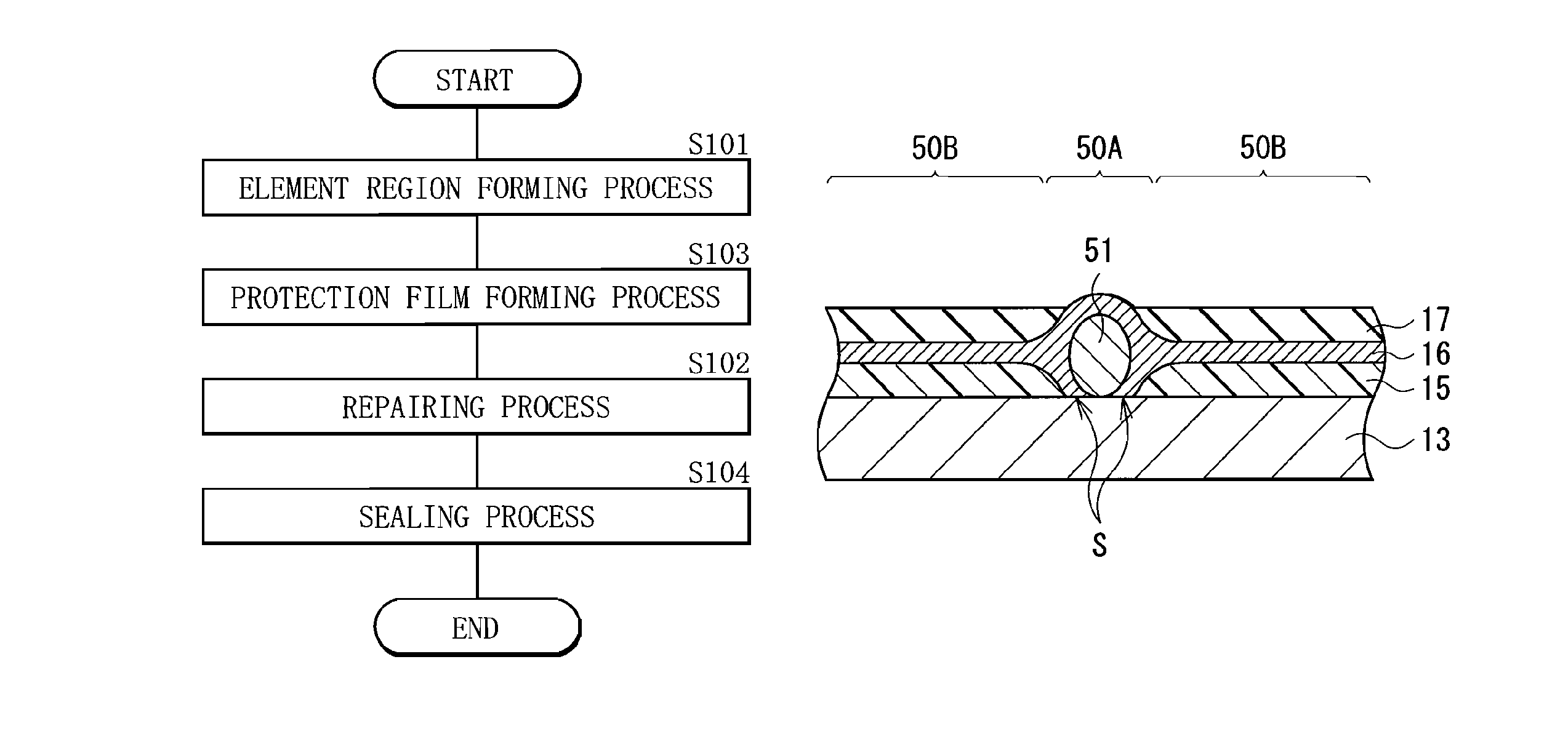
[0068]FIG. 10 shows the flow of a method of manufacturing an organic light-emitting device of a first modification of the present invention. The first modification is similar to the first embodiment except that, after the element region forming process, at least a part of the protection film 17 is formed before the repairing process, and the same actions and effects are obtained. Therefore, the modification will be described by assigning the same reference numerals to the corresponding components.

Element Region Forming Process (Step S101).

[0069]First, in a manner similar to the first embodiment, over the drive substrate 11, the pixel drive circuit 140 including the drive transistor Tr1 and the element region 110 including the organic electroluminescence elements 10R, 10G, and 10B are formed.

Protection Film Forming Process (Step S103)

[0070]Subsequently, for example, by the CVD method, the protection film 17 made of the above-described material is formed. The thickness of the protecti...

second embodiment

[0074]FIG. 12 shows the flow of a method of manufacturing an organic light-emitting device of a second embodiment of the present invention. The second embodiment is similar to the first embodiment except for the repairing process, and the actions and effects of the second embodiment are the same as those of the first embodiment. Therefore, the second embodiment will be described by assigning the same reference numerals to the corresponding components.

Element Region Forming Process (Step S101).

[0075]First, in a manner similar to the first embodiment, over the drive substrate 11, the pixel drive circuit 140 including the drive transistor Tr1 and the element region 110 including the organic electroluminescence elements 10R, 10G, and 10B are formed.

Repairing Process (Step S202)

[0076]Subsequently, as shown in FIG. 13, the element region 110 is temporarily sealed by using a seal layer 51 and a shield substrate 52.

[0077]First, by applying an adhesive resin or sticky region to the periphery...


PUM


Abstract

The present invention provides a method of manufacturing an organic light-emitting device which is applicable to a large-screen display device. The method includes the steps of: forming, over a drive substrate, an element region including a drive transistor, and an organic electroluminescence element in which, an anode, an organic layer and a cathode are stacked in this order; and after the formation of the element region, repairing a short circuit area while setting at least the element region in an atmosphere in which an oxygen concentration is 0.1% or higher and less than 1% and a dew point is −50 degrees or less, and applying a voltage across the anode and the cathode.

Description

CROSS REFERENCE TO RELATED APPLICATIONS[0001]The present invention contains subject matter related to Japanese Patent Application JP 2007-329927 filed in the Japanese Patent Office on Dec. 21, 2007, the entire contents of which being incorporated herein by reference.BACKGROUND OF THE INVENTION[0002]1. Field of the Invention[0003]The present invention relates to a method of manufacturing an organic light-emitting device having an organic electroluminescence (EL) element.[0004]2. Description of the Related Art[0005]In recent years, display devices of the next generation are actively developed, and smaller space, higher brightness, lower power consumption, and the like are in demand. As such a display device, attention is being paid to an organic light-emitting device using an organic electroluminescence element. The organic light-emitting device has characteristics such that since it is of a light-emitting type, the view angle is wide, backlight is unnecessary, so that power consumpti...

Claims


Application Information

Patent Timeline
Patent Type & Authority Patents(United States)
IPC IPC(8): H01L21/00
CPCH01L51/56H01L27/3244H01L51/5234H01L51/5237H01L2251/568H01L2227/323H01L2251/5315H01L2251/564H10K59/12H10K50/828H10K50/841H10K2102/3026H10K50/844H10K59/1201H10K71/841H10K71/861H10K71/00H05B33/10H05B33/04
Inventor TAKAGI, KAZUNARIHIRANO, TAKASHI
Owner JOLED INC
Why Eureka
Try Eureka