Photoreceiving circuit

a buffer circuit and photoreceiving technology, applied in the direction of pulse generators, pulse techniques, oscillation generators, etc., can solve problems such as not divulging means, and achieve the effect of reducing the power supply voltage dependence of offset voltage and good power supply voltage dependen

Active Publication Date: 2011-05-17
RENESAS ELECTRONICS CORP
View PDF8 Cites 0 Cited by
  • Summary
  • Abstract
  • Description
  • Claims
  • Application Information

AI Technical Summary

Benefits of technology

[0023]In this manner, the collector voltages of the third and fourth transistors of the first mirror circuit can be configured to depend on the first operating point voltage. This enables to suppress an difference between the collector-emitter voltages due to the power supply voltage variation and reduce the power supply voltage dependence of the offset voltage.
[0025]In this manner, adding the third constant current circuit enables to separately dispose a reference transistor of the first mirror circuit and configure the transistor that is not used as the reference of the first mirror circuit to have the collector voltage depending on the power supply voltage. This enables to inhibit the offset between the collector-emitter voltages due to the power supply voltage variation and reduce the power supply voltage dependence of the offset voltage.
[0026]According to the present invention, it is possible to provide a buffer circuit, capable of eliminating an difference between collector-emitter voltages due to a power supply voltage variation and allowing the offset voltage to have good power supply voltage dependence, and a photoreceiving circuit using the same.

Problems solved by technology

The related example does not disclose means to solve such problem.

Method used


Image

  • Photoreceiving circuit
  • Photoreceiving circuit
  • Photoreceiving circuit

Examples


first exemplary embodiment

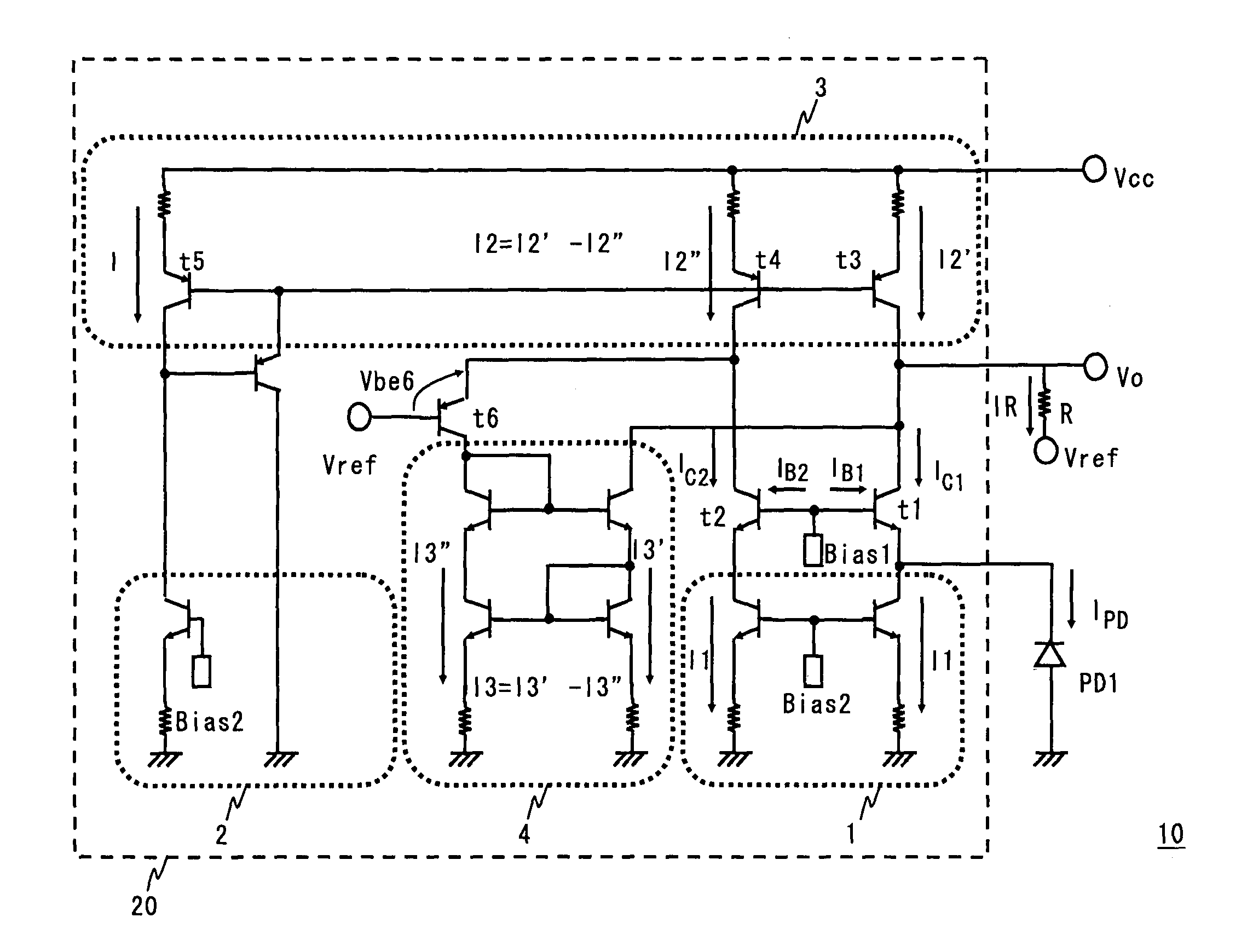
[0036]Referring to FIG. 1, a description is given of a photoreceiving circuit provided with a buffer circuit according to first exemplary embodiment of the present invention. FIG. 1 is a diagram showing a configuration of a photoreceiving circuit 10 provided with a buffer circuit 20 according to the first exemplary embodiment. As shown in FIG. 1, the photoreceiving circuit 10 according to the first exemplary embodiment is provided with a photoreceiving device PD1 and the buffer circuit 20. The buffer circuit 20 includes a first constant current circuit 1, a second constant current circuit 2, a first mirror circuit 3, and a second mirror circuit 4. The present invention relates to a photoreceiving circuit that reduces influence of parasitic capacitance of the photoreceiving device PD (photodiode), which functions as an input source, and that inhibits power supply voltage variation of offset voltage characteristics.

[0037]As shown in FIG. 1, PD1 functioning as an input source is connec...

second exemplary embodiment

[0071]Referring to FIGS. 3 through 5, a description is given of a photoreceiving circuit 10′ using a buffer circuit according to second exemplary embodiment of the present invention. FIG. 3 is a diagram showing a configuration of the photoreceiving circuit 10′ according to the second exemplary embodiment. FIG. 4 is a diagram showing a configuration of a first buffer circuit 21 in FIG. 3, and FIG. 5 is a diagram showing a configuration of a second buffer circuit 22 in FIG. 3. In FIGS. 3 through 5, the same reference numeral is used for an element identical to that of FIG. 1, and the description is omitted as appropriate.

[0072]As shown in FIG. 3, in the photoreceiving circuit 10′, the first buffer circuit 21 is connected to an inverting input terminal (input side) of an I / V conversion operational amplifier 13, which is a differential operational amplifier for current-voltage conversion, and the second buffer circuit 22 is connected to a non-inverting input terminal (reference side). A...

third exemplary embodiment

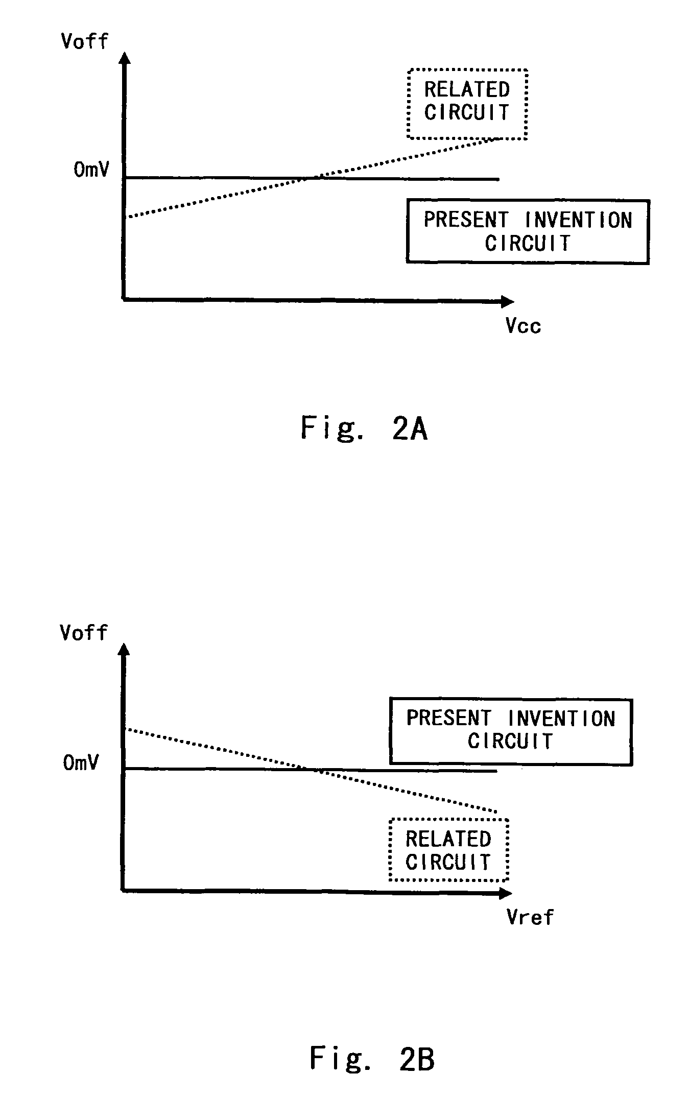
[0075]Referring to FIG. 6, a description is given of a photoreceiving circuit provided with a buffer circuit according to third exemplary embodiment of the present invention. FIG. 6 is a diagram showing a configuration of a photoreceiving circuit 10″ according to the third exemplary embodiment. In the photoreceiving circuit 10″ shown in FIG. 6, although the circuit configuration is approximately equivalent to that of the first exemplary embodiment, improvement is made for the difference between the collector-emitter voltages of the transistors t3 and t4 of the first mirror circuit 3, and further, the photoreceiving circuit 10″ has a configuration of allowing improvements in absolute value of the offset voltage.

[0076]As shown in FIG. 6, in the photoreceiving circuit 10″, an emitter of a transistor t7 is connected to a base of a transistor t6 determining the collector voltage of the transistor t4. In addition, the base voltage of the transistor t7 is voltage Vref.

[0077]In the first ex...


PUM


Abstract

A buffer circuit includes a first transistor (T1) having a base connected to a first power supply, the emitter (E1) and collector (C1) connected as input and output nodes, a second transistor (T2) having a base connected to the first power supply, a first constant current circuit using a difference between outgoing current from E1 and an input current at the current signal input node as a constant current, and determining outgoing current from the emitter of T2 equal to the constant current; and a first mirror circuit equalizing first and second collector currents with a third transistor (T3) with C1 and a fourth transistor (T4) with a collector connected to a collector of T2, a first operating point voltage is provided to the current signal output node between T3 and T1, and a second operating point voltage based on the first operating point voltage between T4 and T2.

Description

BACKGROUND[0001]1. Field of the Invention[0002]The present invention relates to a buffer circuit and a photoreceiving circuit using the same.[0003]2. Description of Related Art[0004]In recent years, recording media such as CDs and DVDs have been widely spread. Such optical recording media are fabricated with dedicated recorders, and techniques are developed daily to improve the recording rate. A photoreceiving IC provided on a pickup unit in such a recorder has a function that converts light reflected from an optical disk into a current with a photoreceiving device and converts it into a voltage signal in a current-voltage conversion circuit. In order to enhance the speed of a recorder, it is required to enhance the speed of a photoreceiving IC used in a pickup unit.[0005]FIG. 7 shows a related circuit diagram disclosed in Japanese unexamined Patent Application Publication No. 60-190011. As shown in FIG. 7, the related example has a configuration in which a PD 2 functioning as an in...

Claims


Application Information

Patent Timeline
Patent Type & Authority Patents(United States)
IPC IPC(8): H02M11/00
CPCH03F3/08
Inventor YANAGI, HIDENOBUIMAI, HITOSHI
Owner RENESAS ELECTRONICS CORP
Why Eureka
Try Eureka