Circuit board unit and method for production thereof

a technology of circuit board and production method, which is applied in the direction of ceramic shaping apparatus, special surfaces, electric devices, etc., can solve the problems of inability to repair partial failures in modules, inability to realize more complex circuits, and inability to realize complex circuits. to achieve the effect of adequate removal of hea

Inactive Publication Date: 2011-05-24
CHARMILLES TECH SA +1
View PDF20 Cites 44 Cited by
  • Summary
  • Abstract
  • Description
  • Claims
  • Application Information

AI Technical Summary

Benefits of technology

[0017]The invention solves this problem with the subject matter of the independent claims, preferred embodiments of the invention are described in the dependent claims.

Problems solved by technology

The disadvantage of this solution is that the degree of integration of the modules is much too small to realize more complex circuits and that a partial failure in a module cannot be repaired.
The heat dissipated by the control electronics may also be considerable, this problem likewise not being solved.
Although modules of this kind are an improvement, they have the disadvantage that they still fail to adequately cool where elevated dissipation is involved, on the one hand, and, on the other are practically non-repairable because the solid backplane represents such a high heat sink that the soldering temperature of leadless solders can hardly be achieved without ruining the circuit in such repair work.
To render the heat-conducting insulation layer effective it is fabricated minimized in thickness which, unfortunately, also results in the disadvantage of high electrical stray capacitances.
The main disadvantages as cited above still remain, but in addition to this, the components towards the center of the circuit boards receive considerably less cooling, because of the limited lateral heat conductivity of the cooling plate, since the heat can only be removed via the edges of the circuit board.
It is interesting that despite the innovation potential of these four patents since their application up to 20 years ago, none of them has found any appreciable acceptance in the marketplace.
There must be reasons for this: firstly reliably segregating the coolant from the electronics of the circuit board (the laminates of which tend to be slightly hygroscopic) is hardly achievable with the methods as proposed, and secondly the cooling capacity of the disclosed solutions is quite simply inadequate for current power applications.
When integrating control electronics and power electronics in a single module, water absorption by the circuit board laminates is particularly fatal.
Water with its relative dielectric constant ∈R=80 results even in small amounts in the stray capacitances being multiplied to disadvantage with catastrophical consequences in view of the currently popular high clock frequencies.
On top of this, water absorption elevates conductivites and thus stray currents ruining e.g. high-impedance analog circuits and insulation barriers.
The corrosion of metallic parts and moldy deposits on non-metallic parts of the circuit board are further negative consequences of water absorption.
Although alternative coolants are proposed in these patents, the cooling capacity is then even further drastically reduced and problems with environment compatability can materialize.

Method used


Image

  • Circuit board unit and method for production thereof
  • Circuit board unit and method for production thereof
  • Circuit board unit and method for production thereof

Examples


first embodiment

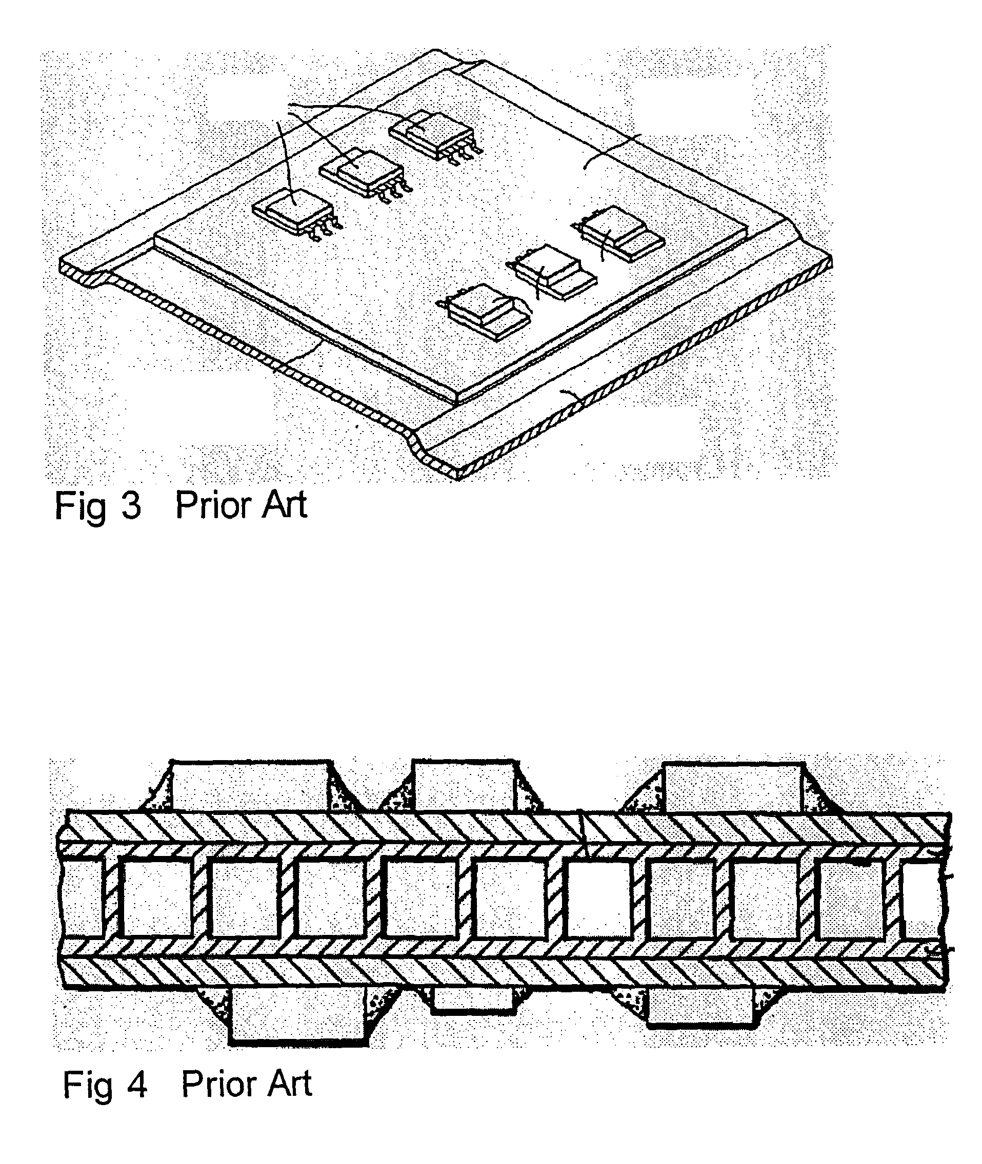
[0060]The advantage of this first embodiment for a power module is a hermetically sealed package simply by adding sidewalls 22 and structural parts 32, 35, 37. The outer surfaces mainly involve cooling plates which effectively prevent heat being dissipated to the environment. Currently popular methods are sufficient for fabricating the circuit boards and their soldering.

second embodiment

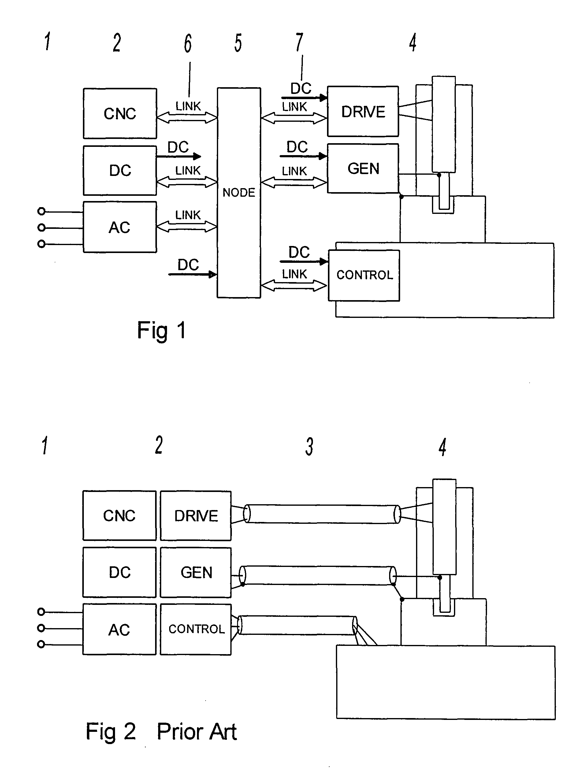
[0061]Referring now to FIG. 8 there is illustrated a power module in which a power board 26 is backed by a control board 27. This arrangement is of advantage when system packs as shown in FIG. 9 are wanted. In this arrangement, firstly a power module is arranged as shown in FIG. 5, then supplemented by any number of modules as shown in FIG. 8, and finally the system pack completed with a control module as shown in FIG. 6.

[0062]The configuration as shown in FIG. 8 is somewhat problematic because of it involving a module which needs to be soldered two-sidedly. Although this can be done with current technology, any subsequent repair or modification poses difficulties. This is why two alternatives are now proposed. Either the cooling plate 16 is duplicated, i.e. a power board as shown in FIG. 5 and a control board as shown in FIG. 6 assembled back-to-back into a power module for reseparation at any time, or the control board 27 is releasably connected to the cooling plate 16. Since the ...

third embodiment

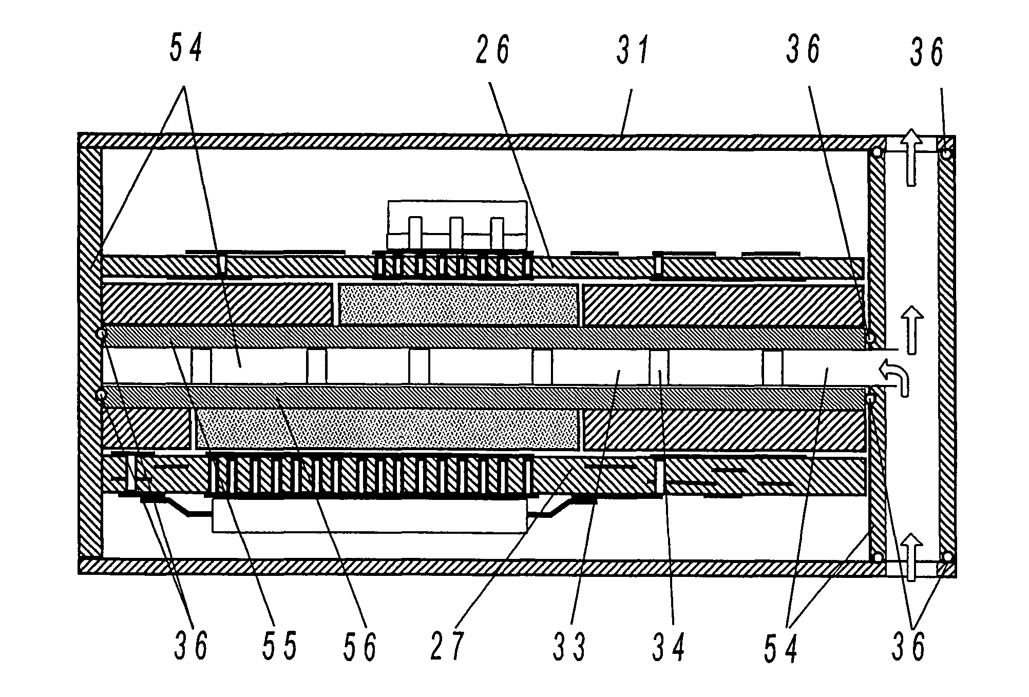
[0073]Referring now to FIG. 10, there is illustrated an even more effective solution. This third embodiment of a module comprises recesses 28 in the cooling plate 16 for interfacing connectors 29. The cooling plate 16 which is preferably made of aluminium or copper is an excellent shield against both electrical and high-frequency magnetic interference. Depending on the SMD profile the connections between the control board 27 and the power board 26 tend to be somewhat shorter.

[0074]The problem of two-sided componenting is in this case the same as in the second embodiment as shown in FIG. 8 and the solutions thereto are likewise the same as proposed by way of FIG. 8. The modules as shown in FIG. 10 can also be stacked into system packs as described above. But the modules should be preferably stacked so that it is always the case that power boards or control boards directly face each other. This saves providing partitioning and just a backplane 30 and a face plane 31 are sufficient for...


PUM

PropertyMeasurementUnit
voltagesaaaaaaaaaa
power lossaaaaaaaaaa

Abstract

The invention relates to a circuit board unit and a method for production thereof. The circuit board unit comprises a circuit board topmost laminate with conductive tracks on the upper side for mounting surface-mountable devices. The circuit board topmost laminate features a thickness dimensioned such that the anticipated heat dissipated by the surface-mountable devices is transported from the upper side to the underside of the circuit board laminate to good effect. The circuit board unit further comprises an electrically insulating laminate arranged under the circuit board topmost laminate, inserts made of a material with good heat conductivity and electrical insulation embedded in the electrically insulating laminate at sites below surface-mountable devices with high heat dissipation, and a cooling plate arranged below the electrically insulating laminate and the inserts.

Description

[0001]The invention relates to a circuit board unit and a method for production thereof, particularly a circuit board unit for removing the heat dissipated by SMDs in power electronic applications.BACKGROUND OF THE INVENTION[0002]Power electronic solutions for objects are increasingly in demand, for example, which formerly, when at all, were achieved with mechanical or electromechanical means. The ever-increasing labor and material costs as well as volume and weight of the electronic assemblies pose the main obstacle for innovative solutions. The tasks making for the most costs are usually manually mounting the power semiconductors and their assembly on cooling devices for evacuating the heat dissipated. The reliability of an assembly is currently dictated practically solely by the quality of these manual working procedures, the quality assurance needed for this purpose adding to the costs involved, however.[0003]Producing, testing, operating and maintenance of such electronic assem...

Claims


Application Information

Patent Timeline
Patent Type & Authority Patents(United States)
IPC IPC(8): H05K7/20
CPCH01L23/3735H05K1/0206B23H1/02B23H11/00H01L23/467Y10T29/49139H01L2924/3011H05K1/0272H05K1/144H05K3/0061H05K2201/0187H05K2201/043H05K2201/10166H01L2924/0002Y10T428/24008H01L2924/00
Inventor BUHLER, ERNSTD'AMARIO, RINOKNAAK, RETO
Owner CHARMILLES TECH SA
Why Eureka
Try Eureka