Implementation of decimation filter in integrated circuit device using ram-based data storage

a technology of integrated circuit devices and data storage, applied in the field of programmable integrated circuits, can solve problems such as the increase in complexity of applications for which plds are used

Active Publication Date: 2011-05-24
ALTERA CORP
View PDF339 Cites 24 Cited by
  • Summary
  • Abstract
  • Description
  • Claims
  • Application Information

AI Technical Summary

Benefits of technology

[0024]FIG. 10 is a simplified block diagram of an illustrative system em

Problems solved by technology

As applications for which PLDs are used increase in complexity, it has become more common to design PLDs

Method used


Image

  • Implementation of decimation filter in integrated circuit device using ram-based data storage
  • Implementation of decimation filter in integrated circuit device using ram-based data storage
  • Implementation of decimation filter in integrated circuit device using ram-based data storage

Examples


Embodiment Construction

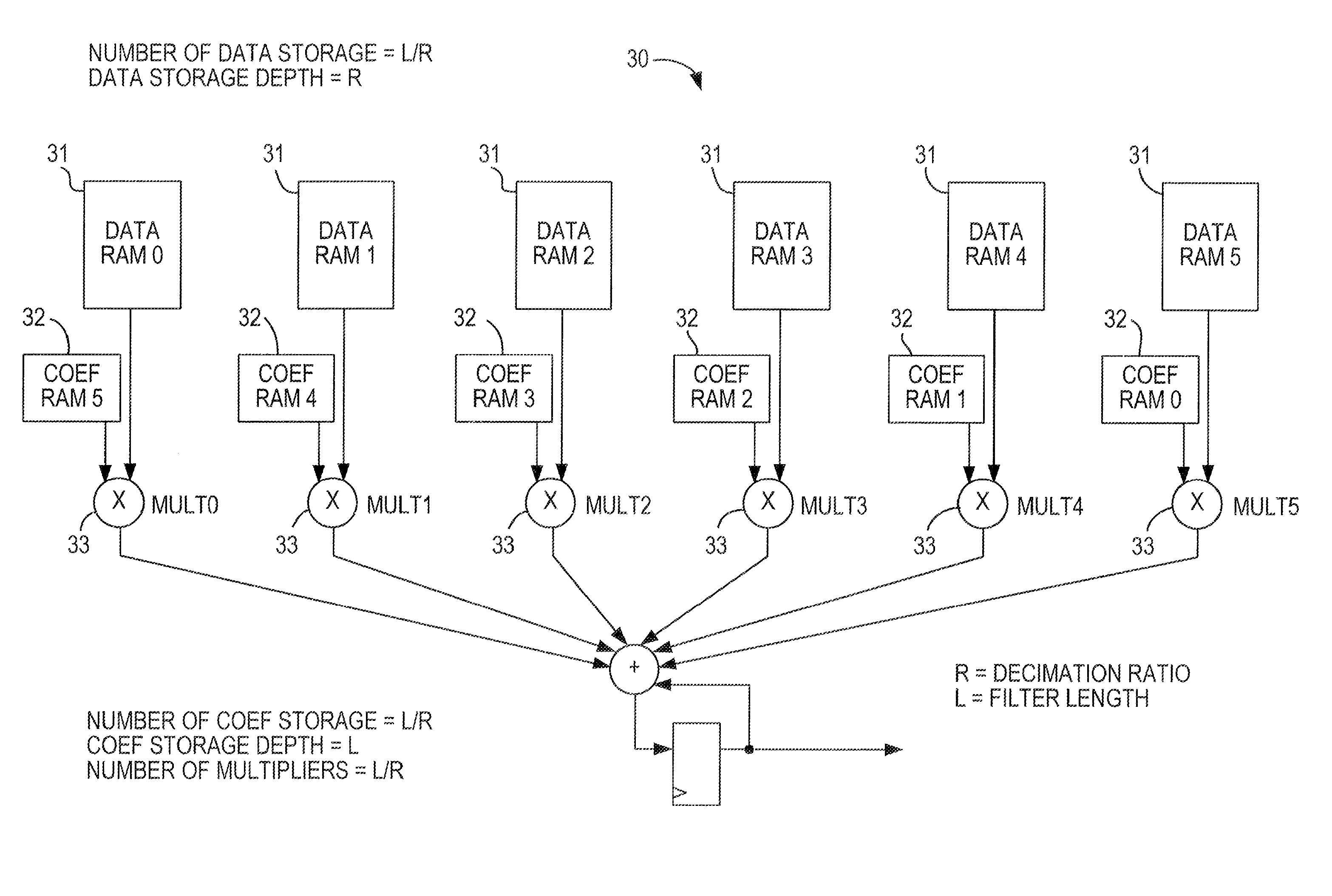
[0027]A FIR filter calculates a weighted sum of a finite number of inputs, summing a number of multiplication results, where each multiplication is between a sample and a coefficient. Each such multiplication may be referred to as a “tap.” Mathematically, a FIR filter may be described as:

[0028]Yk=∑i=0Taps-1⁢ci·sk-i

[0029]where Yk is the kth output term, ci is the ith coefficient, Sk-i is the (k-i)th input sample, and Taps is the number of taps or length of the filter.

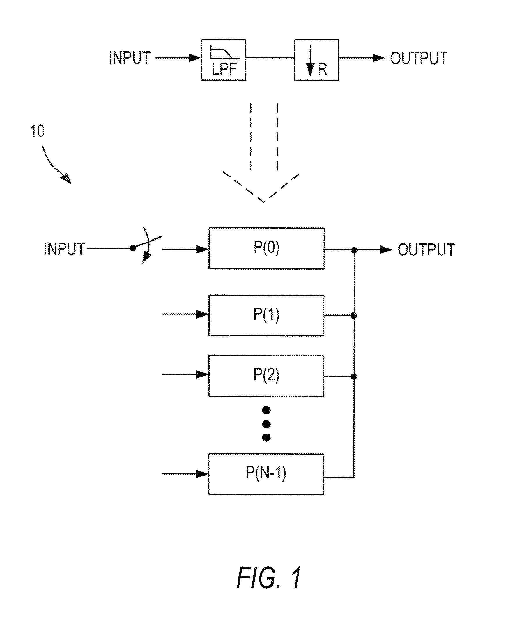
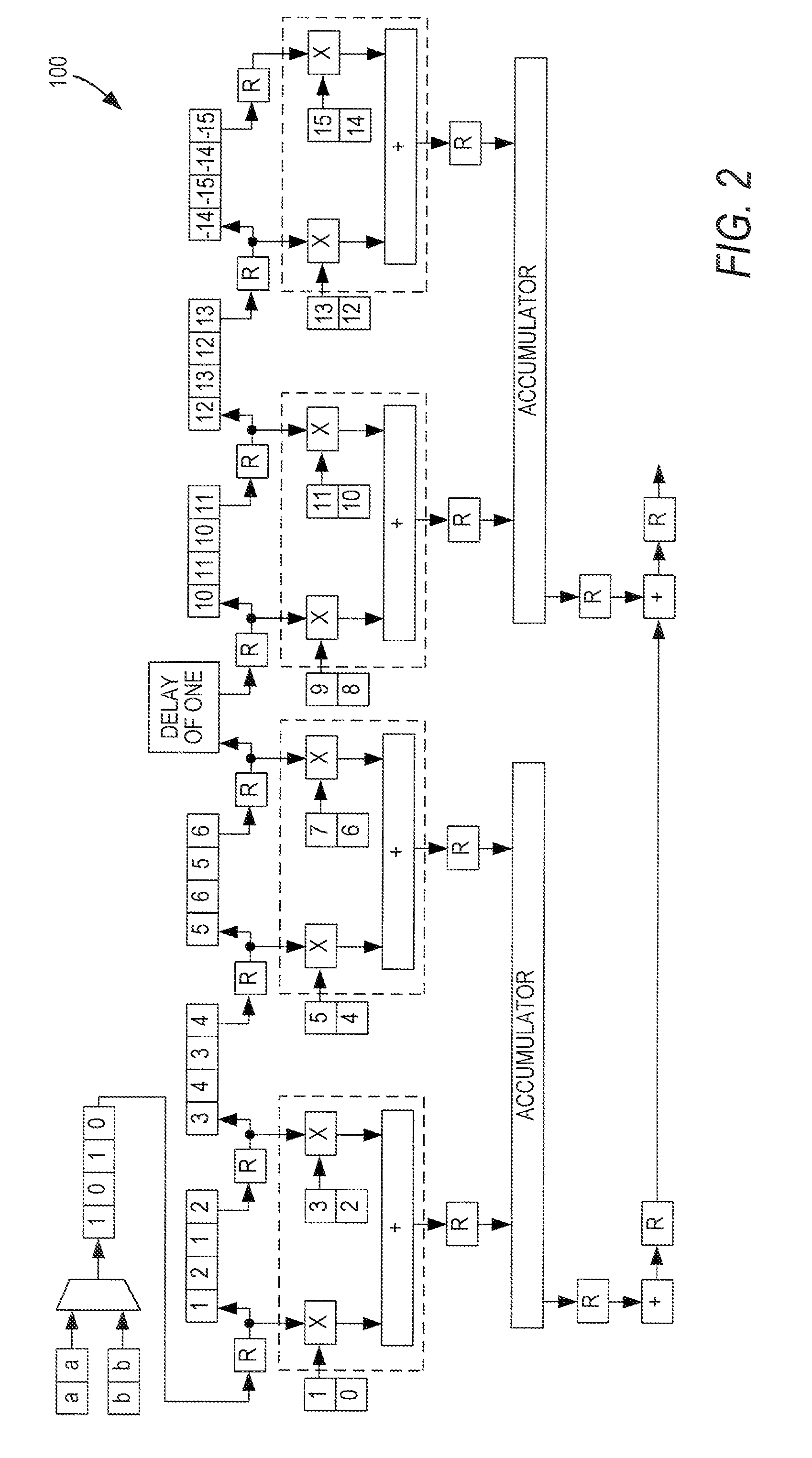
[0030]Decimation filters are used when a signal is resampled at a lower rate. When a high-frequency filter is sampled at a lower rate, data is lost. The higher frequency components may fold back into the signal, so low-pass filtering is needed to prevent distortion of the signal. A generic decimation filter structure 10 is shown in FIG. 1. In this case, the filter preferably is like a multi-channel semi-parallel filter 100 as shown in FIG. 2, with all of the phases being accumulated together. The input is at LF Hz and th...


PUM


Abstract

A programmable integrated circuit device such as a programmable logic device can be configured as a finite impulse response (FIR) filter capable of operating in decimation mode. The device includes at least one user-configurable random access memory block, and that user-configurable random access memory is configured as coefficient memories and data sample memories. The memories are large enough to hold up to all of the coefficients of the filter and a plurality of data samples at one time. Because the data samples and coefficients need not be shifted through the filter at the programmable logic device clock rate, overclocking of the filter is not necessary. The filter can run at a clock rate which is the same as the input data rate, while taking advantage of the available random access memory to mimic a shift register.

Description

BACKGROUND OF THE INVENTION[0001]This invention relates to programmable integrated circuits, such as programmable logic devices (PLDs), and, more particularly, to the implementation of filters in specialized processing blocks which may be included in such devices.[0002]As applications for which PLDs are used increase in complexity, it has become more common to design PLDs to include specialized processing blocks in addition to blocks of generic programmable logic resources. Such specialized processing blocks may include a concentration of circuitry on a PLD that has been partly or fully hardwired to perform one or more specific tasks, such as a logical or a mathematical operation. A specialized processing block may also contain one or more specialized structures, such as an array of configurable memory elements. Examples of structures that are commonly implemented in such specialized processing blocks include: multipliers, arithmetic logic units (ALUs), barrel-shifters, various memo...

Claims


Application Information

Patent Timeline
IPC IPC(8): G06F17/10
CPCH03H17/0223H03H17/0225H03H17/0664H03H2218/085H03H2017/0298
Inventor NEOH, HONG SHANESPOSITO, BENJAMIN
Owner ALTERA CORP
Why Eureka
Try Eureka