Resin filling apparatus, filling method, and method of manufacturing an electronic device

a filling apparatus and resin technology, applied in the field of resin filling apparatus, filling method, and method of manufacturing an electronic device, can solve the problems of affecting reliability, short circuit between adjacent wires, drop in adhesion, etc., and achieve the effect of reducing the entrainment of voids and reducing the filling rate of resin

Inactive Publication Date: 2011-06-07
FUJITSU LTD
View PDF11 Cites 3 Cited by
  • Summary
  • Abstract
  • Description
  • Claims
  • Application Information

AI Technical Summary

Benefits of technology

[0009]The present invention was conceived in view of the problem described above and it is an object of the present invention to provide a resin filling apparatus, a filling method, and a method of manufacturing an electronic device which, when manufacturing an electronic device by filling a cavity between a mounting substrate and an electronic component with resin, can reduce the entrainment of voids during the filling with resin and make it easier for voids entrained in the resin during filling to escape upward. By doing so, there is a further object of manufacturing electronic devices with a significant reduction in entrained voids, reducing the proportion of defective electronic devices, and maintaining high quality.
[0023]According to this method, it is possible to provide a resin filling method where it is easy for voids entrained in resin during filling to escape up an incline and where it is possible to reduce the entrainment of voids by reducing the filling rate of resin.

Problems solved by technology

Conventionally, in an electronic device where the cavity is filled with resin, there has been a problem in that when gaps that have not been filled with resin are present, there is a drop in adhesion, which affects reliability.
For example, when voids (i.e., bubbles entrained in the resin during filling) are present between the bumps and wires, there are problems such as short circuits occurring between adjacent wires due to migration.

Method used


Image

  • Resin filling apparatus, filling method, and method of manufacturing an electronic device
  • Resin filling apparatus, filling method, and method of manufacturing an electronic device
  • Resin filling apparatus, filling method, and method of manufacturing an electronic device

Examples


Embodiment Construction

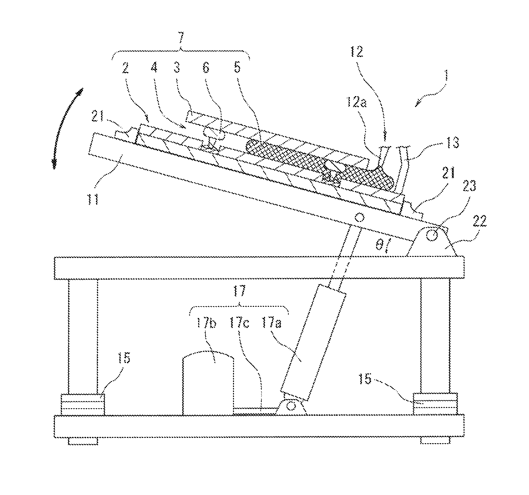
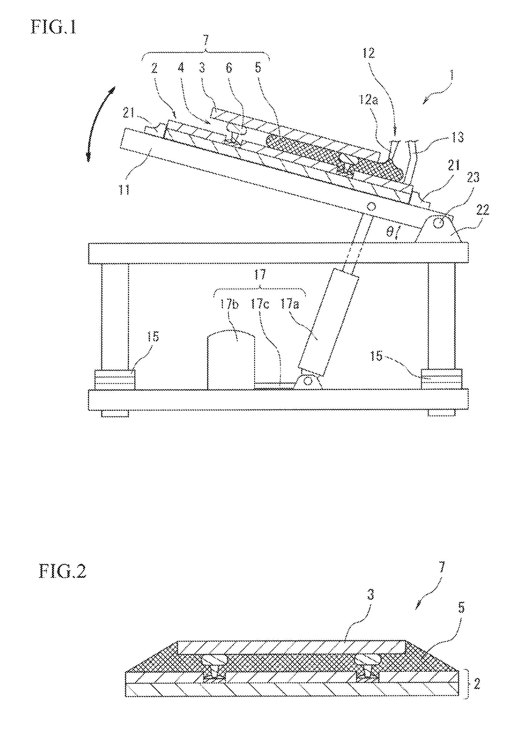
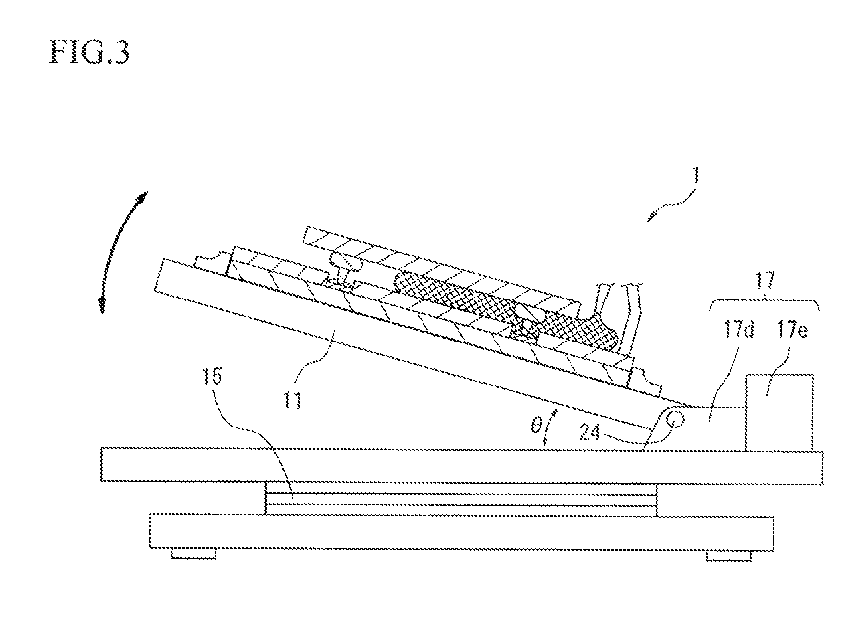
[0030]Embodiments of the present invention will now be described in detail with reference to the drawings. FIG. 1 is a schematic diagram showing one example of a resin filling apparatus 1 according to an embodiment of the present invention. FIG. 2 is a schematic diagram showing one example of an electronic device 7 manufactured according to a method of manufacturing an electronic device according to an embodiment of the present invention. FIG. 3 is a schematic diagram showing another example of a resin filling apparatus 1 according to an embodiment of the present invention. FIGS. 4A and 4B are photographs for comparing an electronic device 7 manufactured according to a method of manufacturing an electronic device according to the present invention and an electronic device 7 manufactured according to the conventional method of manufacturing. Note that in the present specification, the numeral 17 is a general name for the numerals 17a, 17b, . . . in the drawings (this also applies to ...


PUM

PropertyMeasurementUnit
distanceaaaaaaaaaa
inclination angleaaaaaaaaaa
temperatureaaaaaaaaaa

Abstract

A resin filling apparatus, a filling method, and a method of manufacturing an electronic device fill a cavity between a substrate and an electronic component mounted on the substrate with resin. The resin filling apparatus includes a stage for supporting the substrate in an inclined state, and an application head for filling the cavity with resin from a lower side of the inclined substrate.

Description

BACKGROUND OF THE INVENTION[0001]1. Field of the Invention[0002]The present invention relates to a resin filling apparatus that fills resin into a cavity between a substrate and an electronic component mounted on the substrate, to a filling method, and a method of manufacturing an electronic device where a cavity between a substrate and an electronic component mounted on the substrate is filled with resin.[0003]2. Related Art[0004]One example of an electronic device where a cavity between a substrate and an electronic component mounted on the substrate is filled with resin is an electronic device where a semiconductor chip is flip-chip bonded on a mounting substrate.[0005]As shown in FIG. 5, in a conventional method of filling a cavity of this type of electronic device with resin, resin 105 is supplied from a needle 112 to the periphery of a cavity 104 between a substrate 102 and an electronic component 103 while heating the substrate 102 on a hot plate 111 so that the cavity 104 is...

Claims


Application Information

Patent Timeline
Patent Type & Authority Patents(United States)
IPC IPC(8): H01L21/56
CPCH01L21/563H05K3/305H01L2224/73203H05K2201/10674H05K2201/10977H01L2224/92125H01L2224/16225H01L2224/32225H01L2224/73204Y10T29/49002H05K2203/1527H01L2924/00H01L2924/00011H01L2924/00014Y02P70/50H01L2224/0401
Inventor TAKEUCHI, SHUICHI
Owner FUJITSU LTD
Why Eureka
Try Eureka