Method for forming dielectric film using porogen gas

a technology of porogen gas and dielectric film, applied in the field of simiconductor technology, can solve the problems of high cost of apparatus used in curing process after material application, uneven distribution of material,

Active Publication Date: 2011-06-07
ASM JAPAN
View PDF5 Cites 326 Cited by
  • Summary
  • Abstract
  • Description
  • Claims
  • Application Information

AI Technical Summary

Benefits of technology

[0012]Furthermore, use of a silicon hydrocarbon containing multiple alkoxyl groups as a material gas is not without problem, either, although it allows the polymerized oligomer, through optimization of conditions, to form a linear structure like the one demonstrated by siloxane and therefore enables the formation of a porous structure on the silicon substrate and consequently the dielectric constant can be reduced to a desired level. The drawback of this method is that the weak binding power between oligomer molecules in the linear structure results in lower mechanical strength of the film.
[0015]In an embodiment, the purpose of the present invention is to provide a method for forming an insulation film of low dielectric constant easily without increasing the apparatus cost.
[0017]As for the material gas constituted by a silicon hydrocarbon containing multiple crosslinkable groups, in an embodiment of the present invention a compound containing one or more crosslinkable groups can be used alone or combined with a different compound containing one or more crosslinkable groups or with other silicon hydrocarbon. In an embodiment of the present invention, the porogen gas is a hydrocarbon having a linear or cyclic structure and expressed by the general chemical formula CnHm, wherein n is selected from the group of 4 to 14 while m is selected from the group of 4 to 30, and wherein the specific ingredient is selected from the group consisting of α-terpinene, hexane and cyclohexane. In an embodiment of the present invention, the oxidizing gas is selected from the group consisting of O2 and N2O. In an embodiment of the present invention, the inert gas is any one of He, Ar, Kr and Xe or any combination thereof. These gases have different ionizing energy levels and collision cross-section areas, respectively, and therefore use of a different combination of these gases makes it possible to control the reaction occurring in the vapor phase.

Problems solved by technology

However, the conventional approaches mentioned above present the problems described below.
First, in the case of an inorganic SOG insulation film formed by the spin-coat method, the material is not evenly distributed over the silicon substrate, and the apparatus used in the curing process that takes place after the material has been applied is expensive.
Also, a fluorinated amorphous carbon film formed by the plasma CVD method using CxFyHz as a material gas has the drawbacks of the film exhibiting low heat resistance (370° C. or below), poor adhesion with silicon materials, and low mechanical strength.
As a result, a porous structure cannot be formed on the silicon substrate and the dielectric constant cannot be reduced to a desired level.

Method used


Image

  • Method for forming dielectric film using porogen gas
  • Method for forming dielectric film using porogen gas
  • Method for forming dielectric film using porogen gas

Examples


examples

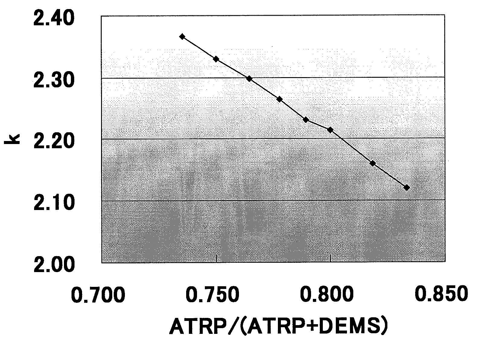
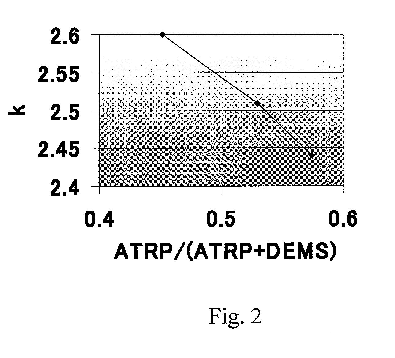
[0049]Controllability of the dielectric constant of the cured insulation film by means of the flow rate of each gas was verified for methods for forming an insulation film of low dielectric constant according to the present invention.

[0050](Experiment 1)

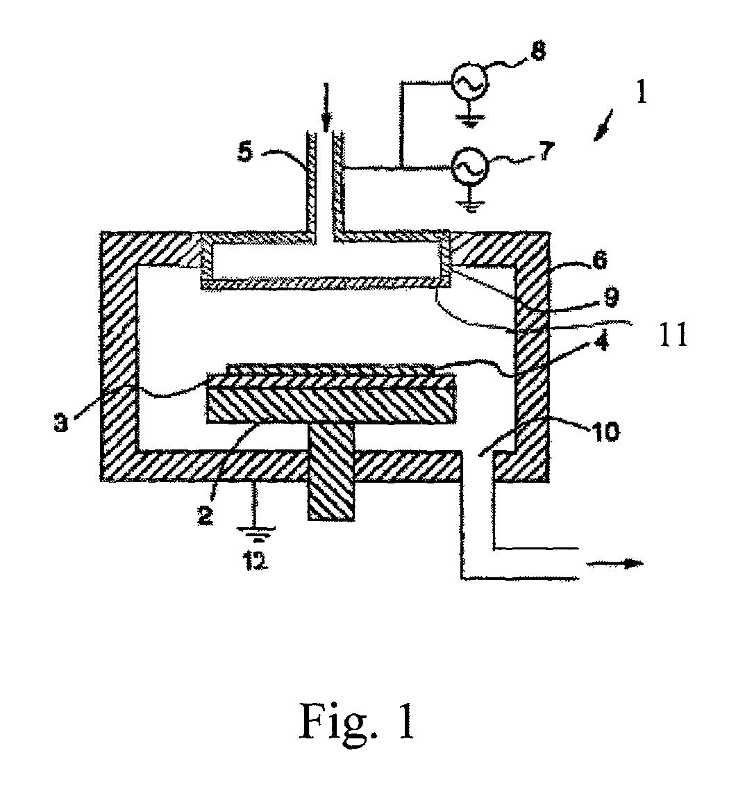
[0051]An experiment was conducted in which an insulation film was formed on a silicon substrate of 300 mm in diameter using the plasma CVD apparatus 1 shown in FIG. 1.

[0052]Conditions for experiment

[0053]A: Material gas: DEMS (diethoxy methyl silane), 73 to 75 sccm

[0054]B: Porogen gas: ATRP (α-terpinene), 60 to 100 sccm

[0055]C: Oxidizing gas: O2, 25 sccm

[0056]D: Inert gas: He, 750 sccm

[0057]First RF power supply: 13.56 MHz, 1.0 W / cm2

[0058]Film forming temperature: 300° C.

[0059]Film forming pressure: 960 Pa

[0060]Film thickness: 500 nm

[0061]Curing method: UV (high-pressure mercury lamp)

[0062]Power: 90 mW / cm2

[0063]Curing temperature: 400° C.

[0064]Curing time: 900 sec

[0065]FIG. 2 shows the relationship between the dielectric constant k...


PUM

PropertyMeasurementUnit
dielectric constantaaaaaaaaaa
temperatureaaaaaaaaaa

Abstract

A method for reducing a dielectric constant of a cured film, includes: introducing a source gas at a flow rate of A, a porogen gas at a flow rate of B, an oxidizing gas at a flow rate of C, and an inert gas into a reaction space in which a substrate is place; increasing a ratio of B / (A+B) used as a parameter for controlling a dielectric constant of a cured film, by a degree substantially or nearly in proportion to a target decrease of dielectric constant of a cured film; applying RF power to the reaction space, thereby depositing a film on the substrate by plasma CVD; and curing the film to remove the porogen material, thereby forming pores in the cured film.

Description

BACKGROUND OF THE INVENTION[0001]1. Field of the Invention[0002]The present invention relates to a semiconductor technology in general. In particular, it relates to a method for forming on a semiconductor substrate a silicon insulation film offering low dielectric constant and achieving high material utilization by using a plasma CVD (chemical vapor deposition) apparatus.[0003]2. Description of the Related Art[0004]The demand for higher, more densely wired semiconductors in recent years is creating a need to reduce inter-wire volumes to prevent signal delays in devices that adopt multi-layer wiring technology. To reduce inter-wire volumes, it is necessary to reduce the dielectric constant of the insulation film formed between adjacent layers in a multi-layer wiring structure. Accordingly, development effort has been made to provide insulation films offering low dielectric constants.[0005]The conventional silicon oxide film SiOx is formed by adding to a silicon material gas such as S...

Claims


Application Information

Patent Timeline
Patent Type & Authority Patents(United States)
IPC IPC(8): C23C16/00
CPCC23C16/401C23C16/56H01L21/02126H01L21/31695H01L21/02216H01L21/02274H01L21/02348H01L21/02203
Inventor TSUJI, NAOTO
Owner ASM JAPAN
Why Eureka
Try Eureka