Wide-band amplifier circuit with improved gain flatness

a wide-band amplifier and gain flatness technology, which is applied in amplifiers with semiconductor devices only, amplifier modifications to extend bandwidth, amplifiers with semiconductor devices, etc., can solve the problems of increasing the chip unit cost, difficult to implement high gain, and expanding the chip size, so as to achieve improved gain flatness and high gain flatness

Inactive Publication Date: 2011-06-07
SAMSUNG ELECTRO MECHANICS CO LTD
View PDF5 Cites 6 Cited by
  • Summary
  • Abstract
  • Description
  • Claims
  • Application Information

AI Technical Summary

Benefits of technology

[0012]An aspect of the present invention provides a wide-band amplifier circuit with improved gain flatness, which satisfies a requirement for a wide band in a band less than 1 GHz in an upload link frequency band in a 3GPP LTE system while having high gain flatness.
[0013]According to an aspect of the present invention, there is provided a wide-band amplifier circuit with improved gain flatness, including: a first resonant load unit connected to an operating power terminal, providing a preset first load, and forming a preset first resonant point; a second resonant load unit connected to the operating power terminal, providing a preset second load, and forming a second resonant point set to a frequency different from the first resonant point; a first amplification unit receiving operating power via the first load of the first resonant load unit, having an amplification band characteristic determined according to the first resonant point of the first resonant load unit, and amplifying an input signal; and a second amplification unit receiving operating power via the second load of the second resonant load unit, having an amplification band characteristic determined according to the second resonant point of the second resonant load unit, and amplifying an input signal from the first amplification unit.
[0019]According to another aspect of the present invention, there is provided a wide-band amplifier circuit with improved gain flatness, including: a first resonant load unit including a first inductance part configured as a bonding pad having one end connected to an operating power terminal, providing a preset first load, and forming a preset first resonant point; a second resonant load unit including a second inductance part configured as a bonding pad having one end connected to the operating power terminal, providing a preset second load, and forming a second resonant point set to a different frequency from the first resonant point; a first amplification unit receiving operating power via the first load of the first resonant load unit, having an amplification band characteristic determined according to the first resonant point of the first resonant load unit, and amplifying an input signal; and a second amplification unit receiving operating power via the second load of the second resonant load unit, having an amplification band characteristic determined according to the second resonant point of the second resonant load unit, and amplifying an input signal from the first amplification unit.

Problems solved by technology

This related art LNA, having the above feedback structure, achieves high linearity, but has limitations in that it is difficult to implement high gain, and additional circuits and currents need to be added for feedback.
This expands the chip size, thereby increasing the unit cost of a chip.

Method used


Image

  • Wide-band amplifier circuit with improved gain flatness
  • Wide-band amplifier circuit with improved gain flatness
  • Wide-band amplifier circuit with improved gain flatness

Examples


Embodiment Construction

[0031]Exemplary embodiments of the present invention will now be described in detail with reference to the accompanying drawings.

[0032]The invention may, however, be embodied in many different forms and should not be construed as being limited to the embodiments set forth herein. Rather, these embodiments are provided so that this disclosure will be thorough and complete, and will fully convey the scope of the invention to those skilled in the art. Like reference numerals in the drawings denote like elements.

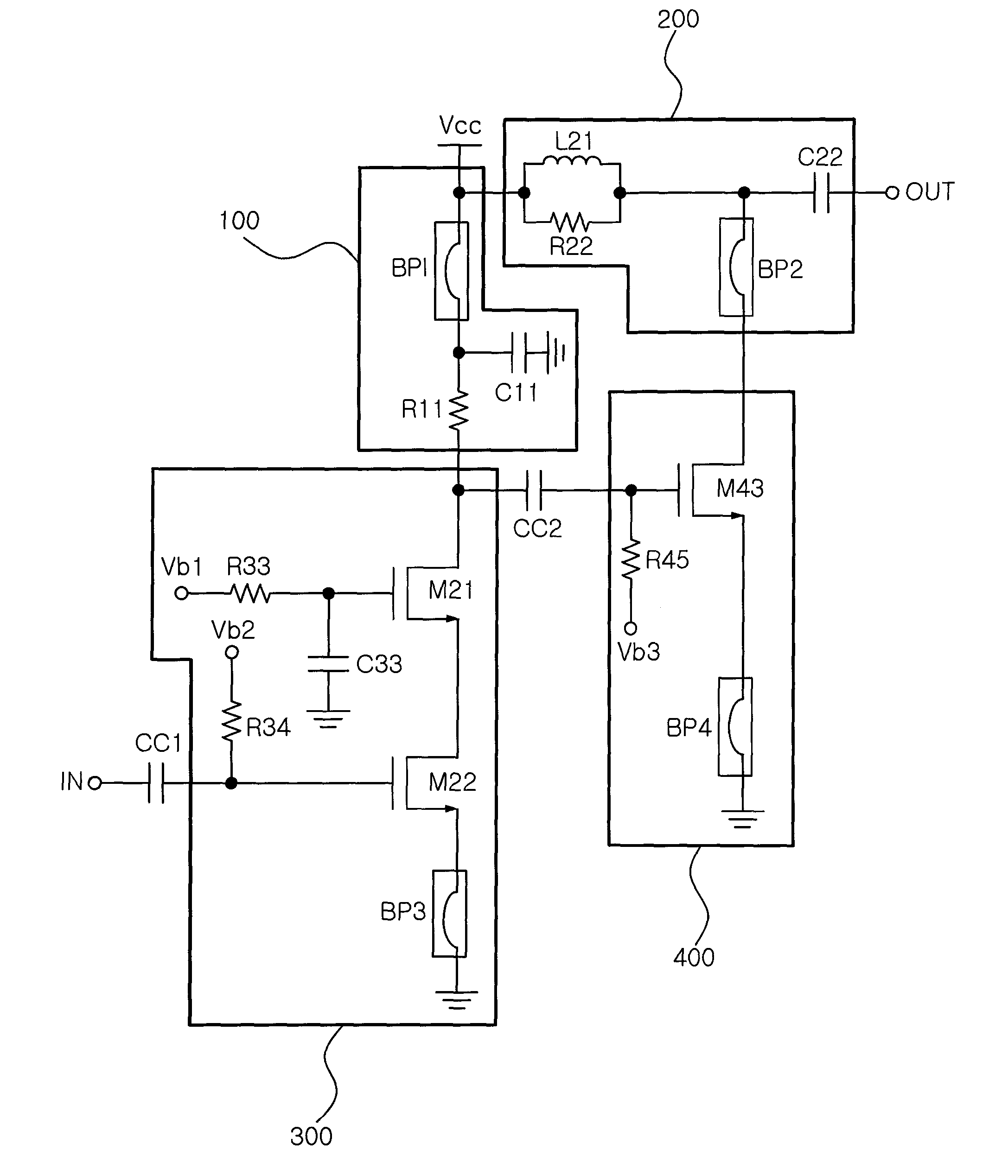
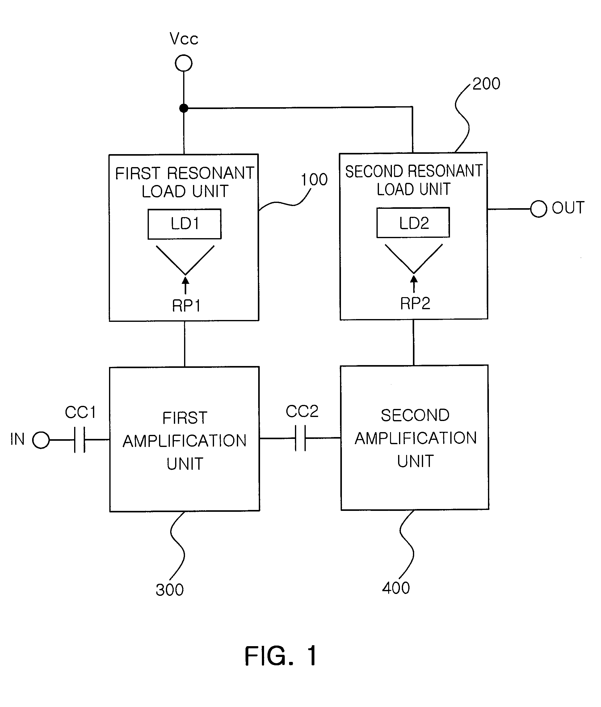
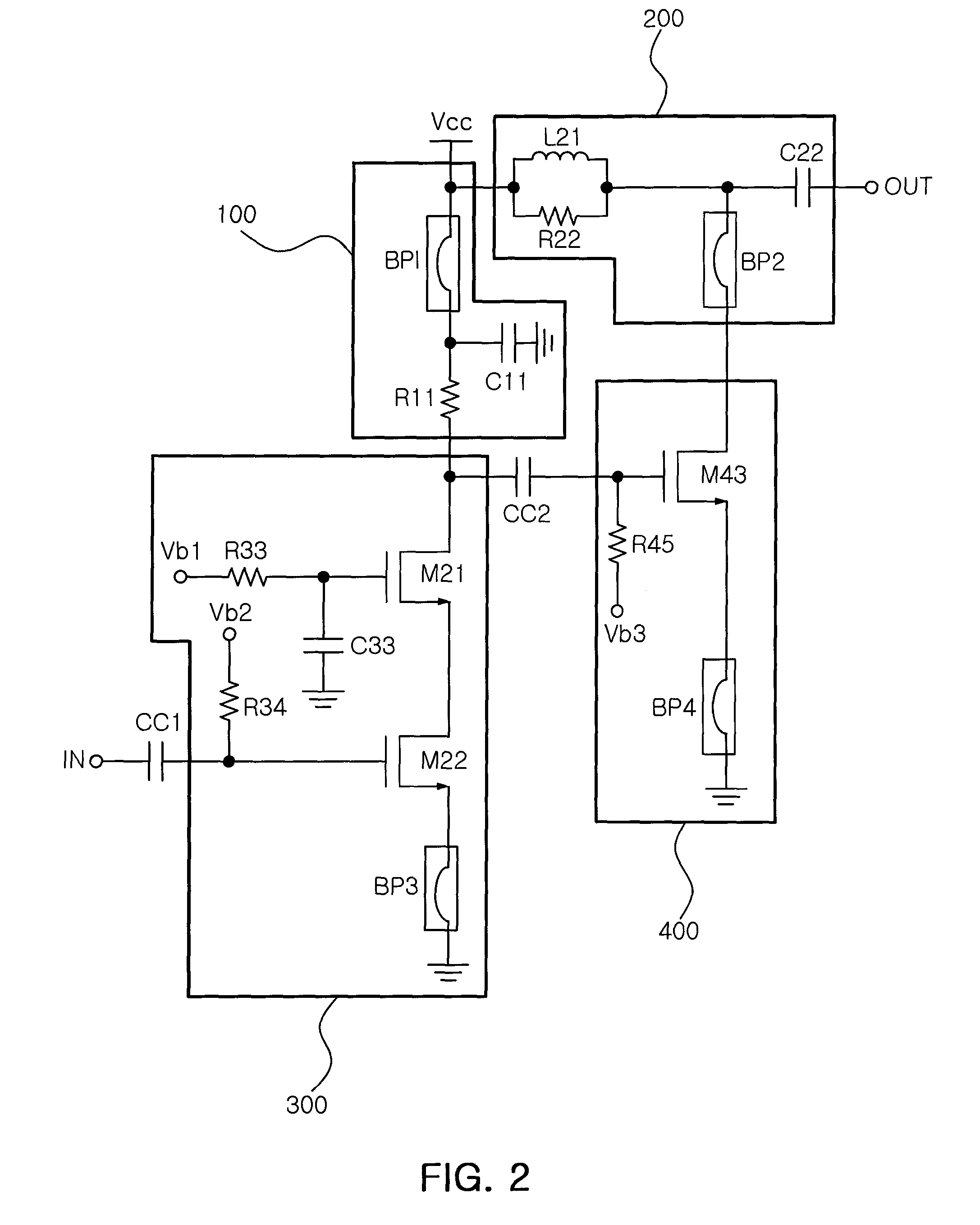
[0033]FIG. 1 is a block diagram of a wide-band amplifier circuit with improved gain flatness, according to an exemplary embodiment of the present invention.

[0034]Referring to FIG. 1, a wide-band amplifier circuit with improved gain flatness, according to an exemplary embodiment of the present invention, includes: a first resonant load unit 100 connected to an operating power terminal Vcc, providing a preset first load LD1, and forming a preset first resonant point RP1; a second ...


PUM


Abstract

There is provided a wide-band amplifier circuit with improved gain flatness. The wide-band amplifier circuit includes a first resonant load unit connected to an operating power terminal, providing a preset first load, and forming a preset first resonant point, a second resonant load unit connected to the operating power terminal, providing a preset second load, and forming a second resonant point set to a frequency different from the first resonant point; a first amplification unit receiving operating power via the first load of the first resonant load unit, having an amplification band characteristic determined according to the first resonant point of the first resonant load unit, and amplifying an input signal; and a second amplification unit receiving operating power via the second load, having an amplification band characteristic determined according to the second resonant point, and amplifying an input signal from the first amplification unit.

Description

CROSS-REFERENCE TO RELATED APPLICATIONS[0001]This application claims the priority of Korean Patent Application No. 10-2009-0051081 filed on Jun. 9, 2009, in the Korean Intellectual Property Office, the disclosure of which is incorporated herein by reference.BACKGROUND OF THE INVENTION[0002]1. Field of the Invention[0003]The present invention relates to a wide-band amplifier circuit with improved gain flatness, which is applicable to a 3rd Generation Partnership Project Long-Term Evolution (3GPP LTE) system, and more particularly, to a wide-band amplifier circuit with improved gain flatness, which satisfies a requirement for a wide band in a band less than 1 GHz in an upload link frequency band while having high gain flatness.[0004]2. Description of the Related Art[0005]3GPP LTE communications systems, considered to be 4G technology, are techniques that aim at supporting various services based on packet data transfer. The 3GPP LTE communications systems support a downlink peak data r...

Claims


Application Information

Patent Timeline
Patent Type & Authority Patents(United States)
IPC IPC(8): H03F3/191
CPCH03F1/42H03F2200/36H03F1/08
Inventor JEONG, MOON SUKNA, YOO SAM
Owner SAMSUNG ELECTRO MECHANICS CO LTD
Why Eureka
Try Eureka