

Transparent conductor
a conductor and transparent technology, applied in the direction of non-metal conductors, conductive layers on insulating supports, instruments, etc., can solve the problems of varying electric resistance, and achieve the effect of sufficient transparency and adequate suppression of electric resistance variation
- Summary
- Abstract
- Description
- Claims
- Application Information
AI Technical Summary
Benefits of technology
Problems solved by technology
Method used
Image

Examples
first embodiment
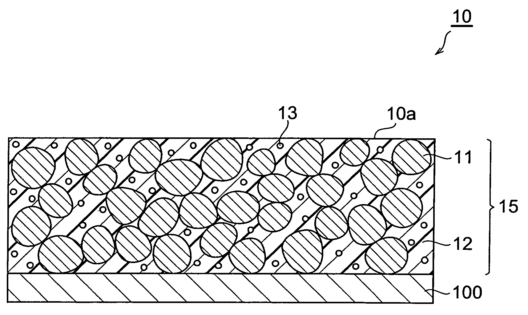
[0031]First, the first embodiment of the transparent conductor of the present invention will be described.
[0032]FIG. 1 is a schematic sectional view showing the first embodiment of the transparent conductor according to the present invention. As shown in FIG. 1, the transparent conductor 10 of the present embodiment has an electrically conductive layer 15 and a substrate 100, and the electrically conductive layer 15 is laid on the substrate 100. The conductive layer 15 is comprised of electrically conductive particles 11, a binder 12, and an ultraviolet absorber 13. The electrically conductive particles 11 are filled inside the conductive layer 15, and the conductive particles 11 and the ultraviolet absorber 13 are fixed in the binder 12. Here the ultraviolet absorber 13 is not chemically bound to the binder 12, but is dispersed in the binder.
[0033]In the transparent conductor 10, preferably, the conductive particles 11 are in contact with each other and some of conductive particles...
second embodiment
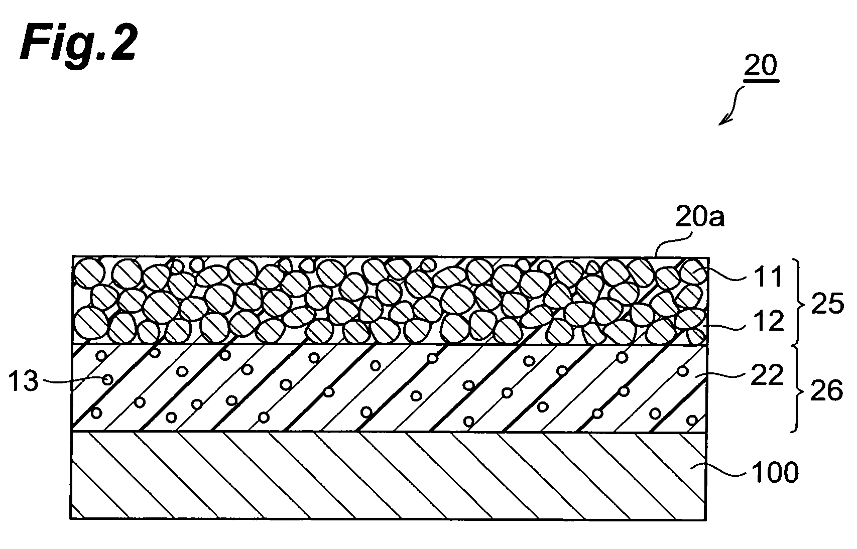
[0080]Next, the second embodiment of the transparent conductor according to the present invention will be described.
[0081]FIG. 2 is a schematic sectional view showing the second embodiment of the transparent conductor according to the present invention. As shown in FIG. 2, the transparent conductor 20 of the present embodiment has an electrically conductive layer 25 containing electrically conductive particles 11 and a binder 12, an ultraviolet absorbing layer 26 containing an ultraviolet absorber 13, and a substrate 100, and the ultraviolet absorbing layer 26 and the conductive layer 25 are stacked in this order on the substrate 100. The conductive particles 11 are filled inside the conductive layer 25 and the conductive particles 11 are fixed in the binder 12.
[0082]In the transparent conductor 20, preferably, the conductive particles 11 are in contact with each other and some of conductive particles 11 are exposed in a surface 20a of the transparent conductor 20. In this case, the...
third embodiment
[0108]Next, the third embodiment of the transparent conductor according to the present invention will be described. The transparent conductor 30 of the third embodiment is different from the first embodiment in that an ultraviolet absorbing binder 32 is used instead of the binder 12 and ultraviolet absorber 13.
[0109]FIG. 3 is a schematic sectional view showing the third embodiment of the transparent conductor according to the present invention. As shown in FIG. 3, the transparent conductor 30 of the present embodiment has an electrically conductive layer 35 and a substrate 100, and the conductive layer 35 is laid on the substrate 100. The conductive layer 35 has electrically conductive particles 11 and the ultraviolet absorbing binder 32. The electrically conductive particles 11 are filled inside the conductive layer 35 and the electrically conductive particles 11 are fixed in the ultraviolet absorbing binder 32.
[0110]In the transparent conductor 30, preferably, the conductive parti...
PUM
| Property | Measurement | Unit |
|---|---|---|
| thickness | aaaaa | aaaaa |
| thickness | aaaaa | aaaaa |
| grain size | aaaaa | aaaaa |
Abstract
Description
Claims
Application Information