Method for manufacturing device

a manufacturing method and technology of a manufacturing device, applied in the field of manufacturing a device, can solve the problems of inability to mount adhesive film for die bonding, inability to reliably prevent chipping on the back side of the device, and inability to carry out bonding operation smoothly, so as to achieve the effect of reliably preventing chipping

Active Publication Date: 2011-06-14
DISCO CORP
View PDF4 Cites 0 Cited by
  • Summary
  • Abstract
  • Description
  • Claims
  • Application Information

AI Technical Summary

Benefits of technology

[0009]It is an object of the present invention to provide a method for manufacturing a device, the device having an adhesive film for die bonding mounted on the back side of the device, without lowering the quality of the device.
[0018]According to the present invention, when the wafer severing step is carried out, the uncut portion remains on the front side of the wafer, so that the cutting grooves are kept straight. Thus, the wafer can be cut along the cutting grooves by the cutting blade. In the wafer severing step, moreover, chipping does not occur at the back side of the divided device, since the cutting grooves have already been formed during the cutting groove forming step in the back side of the wafer in the regions to be cut by the cutting blade. Particularly in case the thickness of the cutting blade for performing the wafer severing step is thinner than the thickness of the cutting blade which has performed the cutting groove forming step, the cutting blade does not contact the surroundings of the back side of the device to be cut. Thus, chipping can be reliably prevented from occurring in the back side of the device.

Problems solved by technology

However, severing the adhesive film, together with the semiconductor wafer, by the cutting blade to divide the wafer into the individual devices poses the problem that chipping occurs in the back side of the device.
Thus, the adhesive film for die bonding cannot be mounted, beforehand, on the back side of the semiconductor wafer.
Hence, when the device produced by the DBG method is bonded to the die bonding frame, this bonding has to be performed, with a bonding agent being inserted between the device and the die bonding frame, thus arousing the problem that a bonding operation cannot be carried out smoothly.
It is difficult to relatively move the cutter, which has bee inserted into the division grooves, along the contorted division grooves.
It is also difficult to perform irradiation with the laser beam along the contorted division grooves.

Method used


Image

  • Method for manufacturing device
  • Method for manufacturing device
  • Method for manufacturing device

Examples


Embodiment Construction

[0029]Preferred embodiments of the method for manufacturing a device in accordance with the present invention will be described in detail by reference to the accompanying drawings.

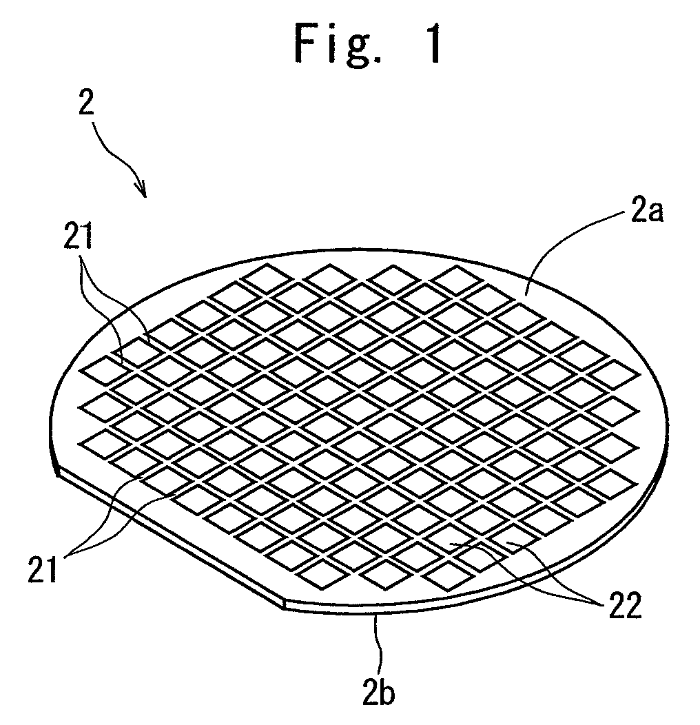
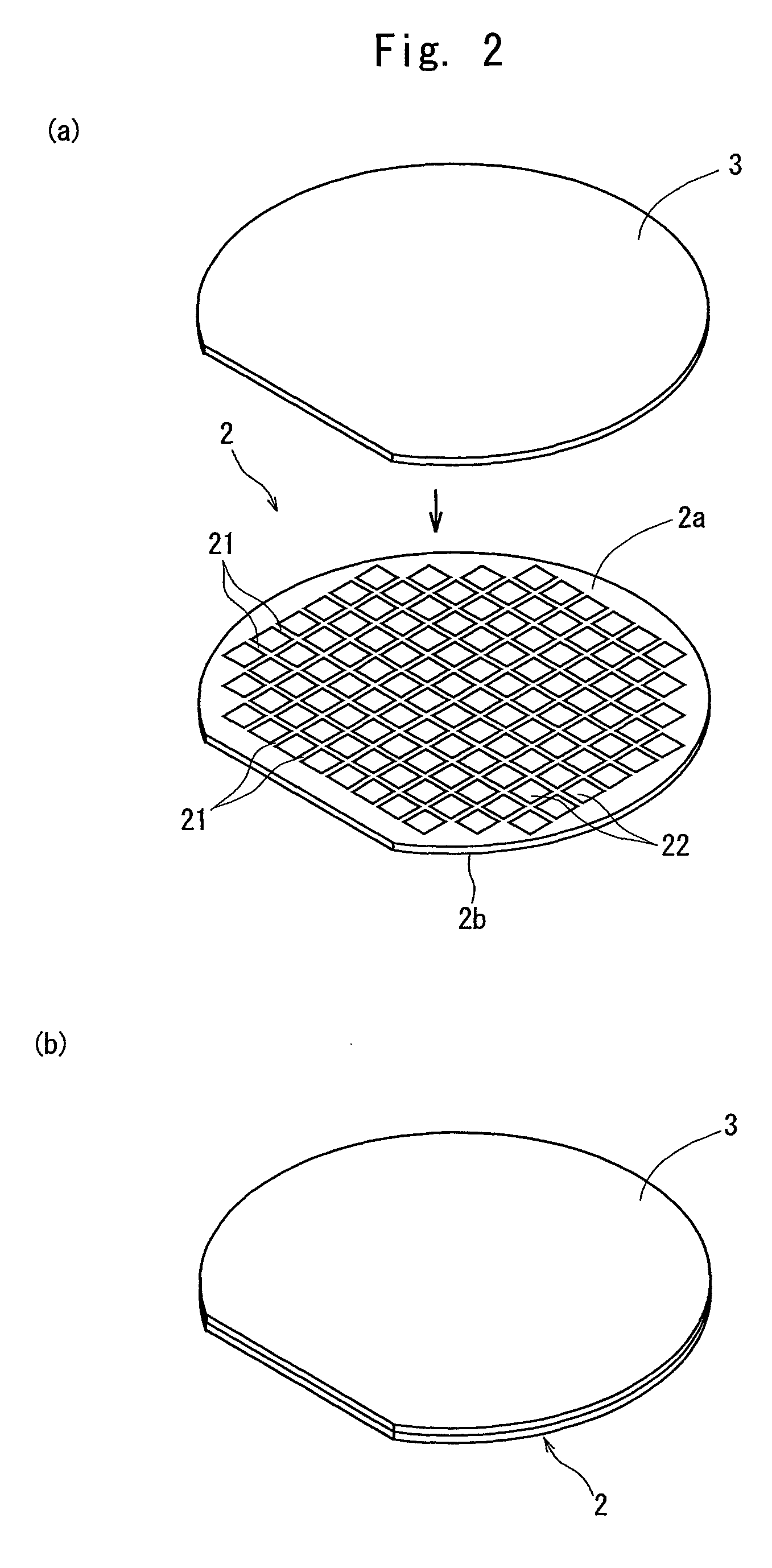
[0030]FIG. 1 shows a perspective view of a semiconductor wafer as a wafer. A semiconductor wafer 2 shown in FIG. 1 comprises, for example, a silicon wafer having a thickness of 700 μm, and a plurality of predetermined division lines 21 are formed in a lattice pattern on the surface 2a of the semiconductor wafer 2. On the surface 2a of the semiconductor wafer 2, devices 22, such as IC's or LSI's, are formed in a plurality of regions defined by the plurality of predetermined division lines 21 formed in the lattice pattern.

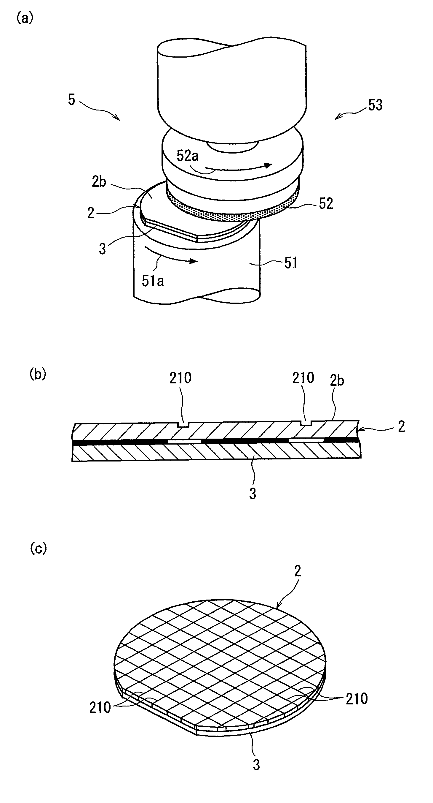
[0031]To produce the individual devices by dividing the above-mentioned semiconductor wafer 2 along the predetermined division lines 21, a first step is to stick a protective tape 3 to the surface 2a of the semiconductor wafer 2 (i.e., the surface where the devices 22 are formed), as shown ...


PUM

PropertyMeasurementUnit
thicknessaaaaaaaaaa
thicknessaaaaaaaaaa
thicknessaaaaaaaaaa

Abstract

A method for manufacturing a device, in which a wafer having a plurality of devices formed on the face thereof is divided into the individual devices, and an adhesive film is mounted on the back side of each device. This method comprises: a cutting groove forming step of cutting the back side of the wafer along predetermined division lines by a cutting blade to form cutting grooves, while leaving an uncut portion, which is thinner than the target thickness of the device, on the front side of the wafer; a back side grinding step of grinding the back side of the wafer to the target thickness of the device, while allowing the cutting grooves to remain in the back side of the wafer; an adhesive film mounting step of mounting an adhesive film to the back side of the wafer; a wafer supporting step of sticking the adhesive film side of the wafer, on which the adhesive film has been mounted, to the surface of a dicing tape; a wafer severing step of cutting the front side of the wafer along the predetermined division lines by a cutting blade to sever the uncut portion, thereby dividing the wafer into the individual devices and cutting the adhesive film; and an adhesive film separating step of expanding the dicing tape to separate the adhesive film per device.

Description

FIELD OF THE INVENTION[0001]This invention relates to a method for manufacturing a device, by which a wafer having devices formed in a plurality of regions defined by predetermined division lines formed in a lattice pattern on the surface of the wafer is divided into the individual devices along the predetermined division lines, and an adhesive film for die bonding is mounted on the back side of each device.DESCRIPTION OF THE PRIOR ART[0002]In a semiconductor device manufacturing process, for example, devices, such as IC's and LSI's, are formed in a plurality of regions defined by streets (predetermined division lines) formed in a lattice pattern on the surface of a nearly disk-shaped semiconductor wafer, and the respective regions having the devices formed therein are divided along the predetermined division lines to produce the individual devices. A cutting apparatus, called a dicing apparatus, is generally used as a dividing apparatus for dividing the semiconductor wafer. This cu...

Claims


Application Information

Patent Timeline
Patent Type & Authority Patents(United States)
IPC IPC(8): H01L21/46
CPCB28D5/0082B32B38/0004H01L21/78H01L21/67132B32B38/0012B32B37/12B32B2457/08
Inventor SEKIYA, KAZUMA
Owner DISCO CORP
Why Eureka
Try Eureka