

CMOS image sensor with interpolated data of pixels
a technology of image sensor and pixels, applied in the field of cmos image sensor, can solve the problems of deteriorating sensitivity, increasing delay of control signal, and differing horizontal and vertical resolutions, and achieves the effect of doubling resolution, maintaining sensitivity, and easy interpolation
- Summary
- Abstract
- Description
- Claims
- Application Information
AI Technical Summary
Benefits of technology
Problems solved by technology
Method used
Image

Examples
Embodiment Construction
[0035]Hereinafter, embodiments of the present invention will be described in detail with reference to the attached drawings.
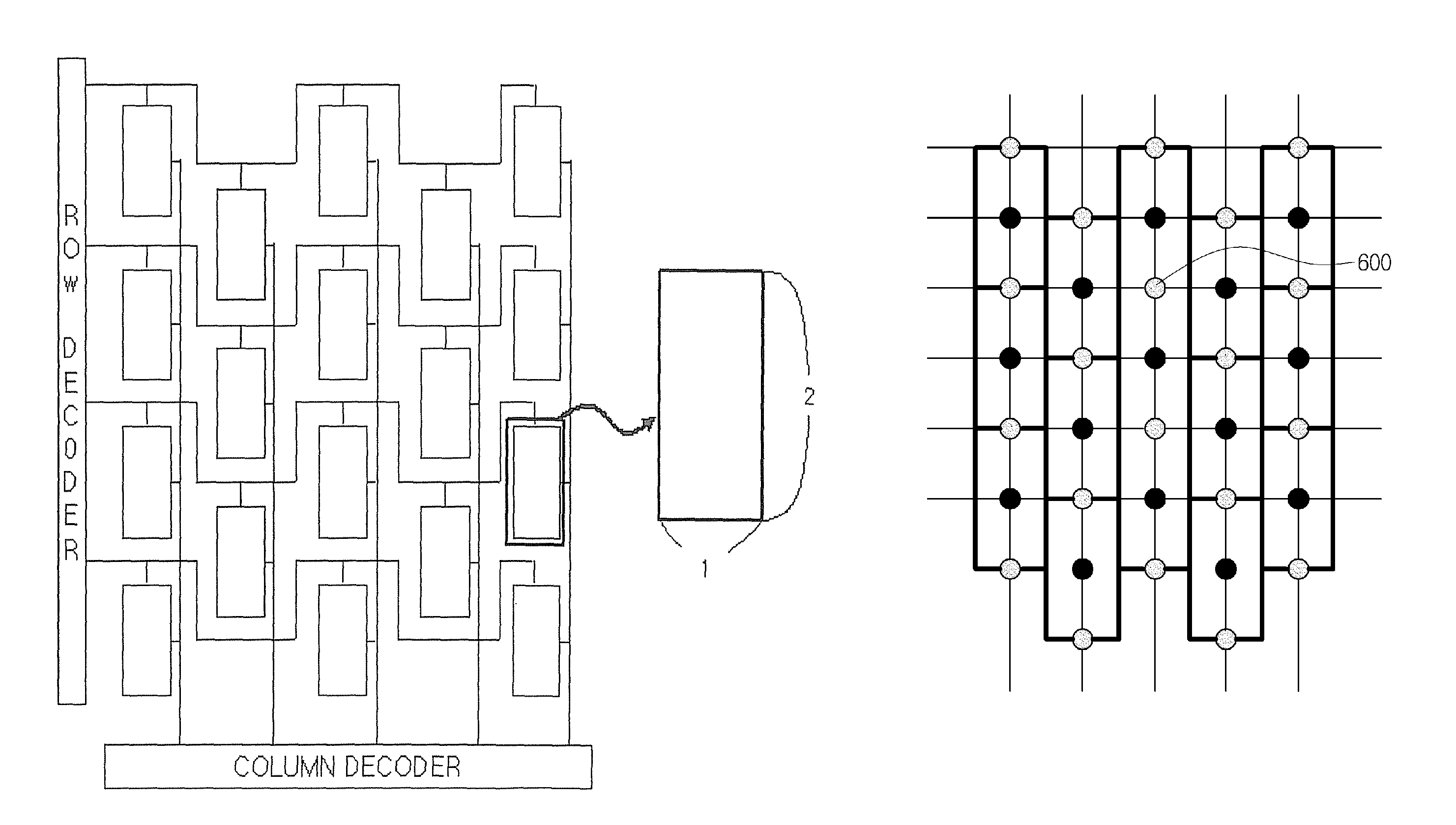
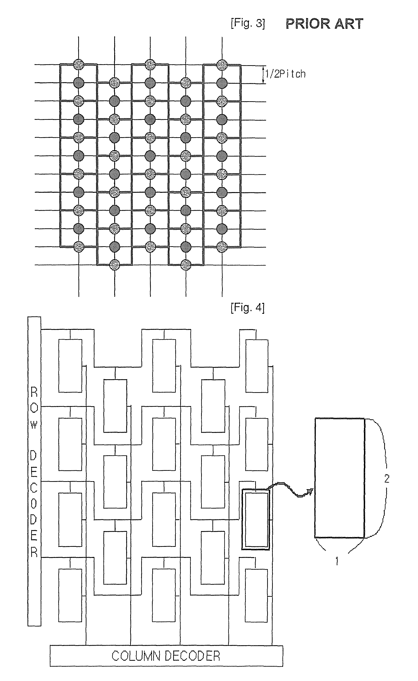
[0036]FIG. 4 is a view showing an image sensor having rectangular unit pixels according to an embodiment of the present invention.
[0037]As shown in FIG. 4, the image sensor of the present invention has rectangular unit pixels each having a width to length ratio of 1:2. As a result, the image sensor of the present invention can maintain the same resolution in horizontal and vertical directions.
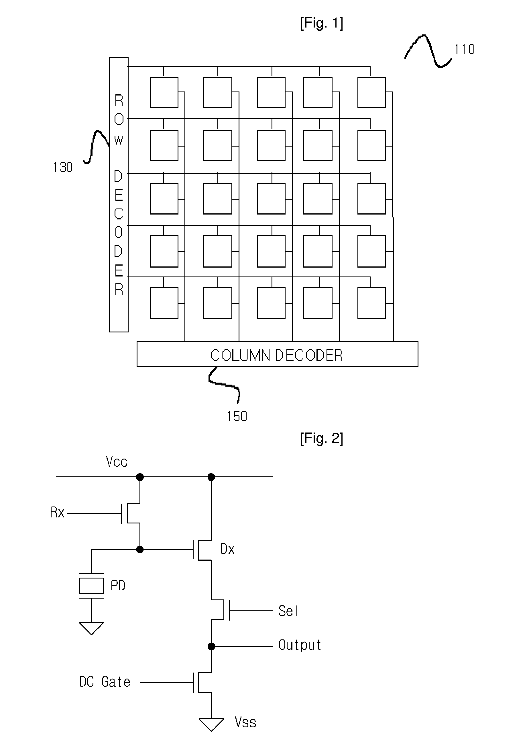
[0038]FIG. 5 is a block diagram showing an image processing apparatus including an image sensor having rectangular unit pixels according to the present invention. Referring to FIG. 5, the image processing apparatus includes a CMOS image sensor 510, an image processing unit 520, a display unit 530 and a control unit 540. In detail, the CMOS image sensor 510 is constructed so that a plurality of pixels each having a width to length ratio of 1:2 is arranged in a two-dimension...
PUM
 Abstract
Description
Claims
Application Information