

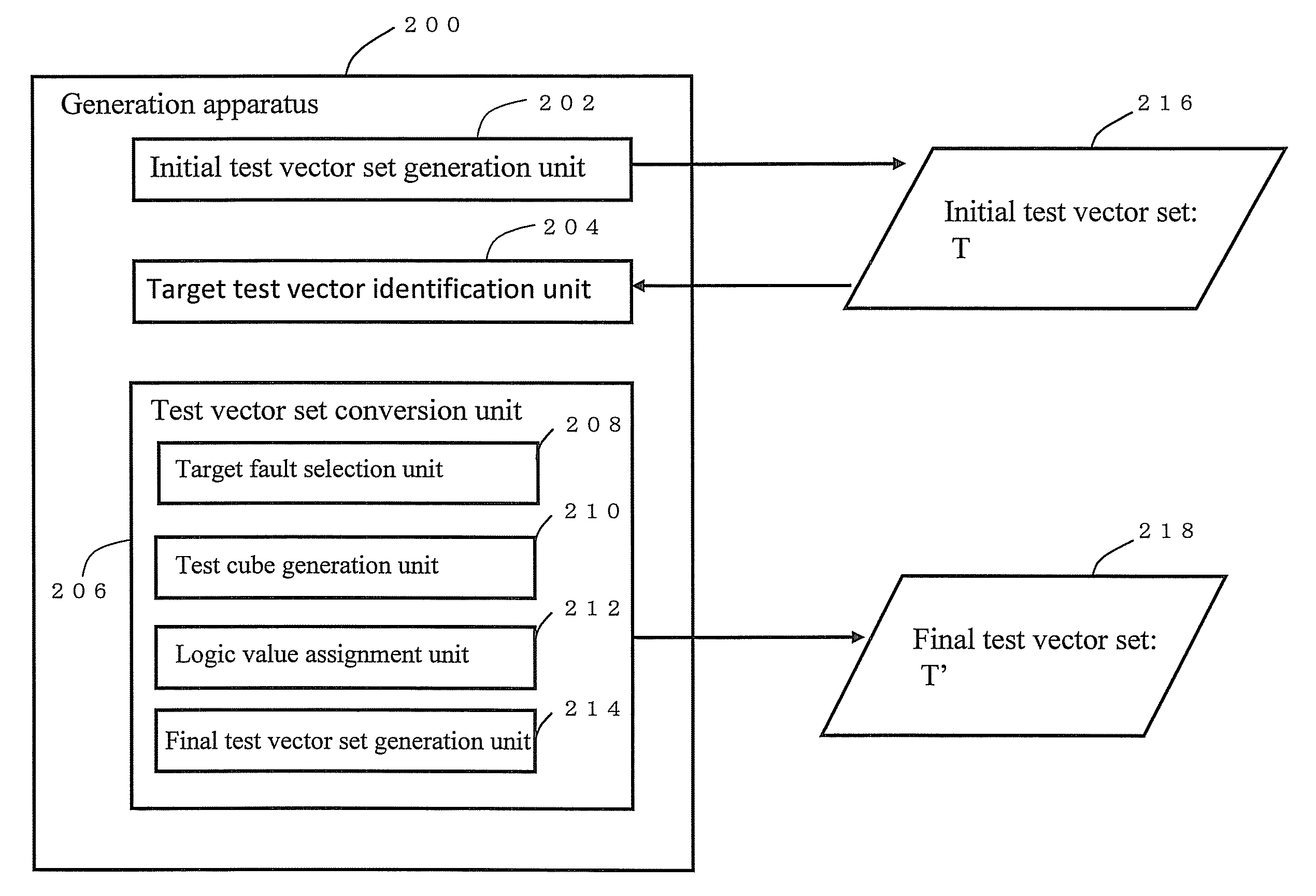
Generating device, generating method, program and recording medium
a generating device and a technology for recording media, applied in measurement devices, instruments, computing, etc., can solve the problems of controllability over the pseudo primary input line and the observation of the pseudo primary output line, and achieve the effect of reducing the differences in the generated logic value, avoiding faulted test results, and suppressing scan capture power dissipation
- Summary
- Abstract
- Description
- Claims
- Application Information
AI Technical Summary
Benefits of technology
Problems solved by technology
Method used
Image

Examples
Embodiment Construction
[0056]Hereinafter, embodiments of the present invention will be described.
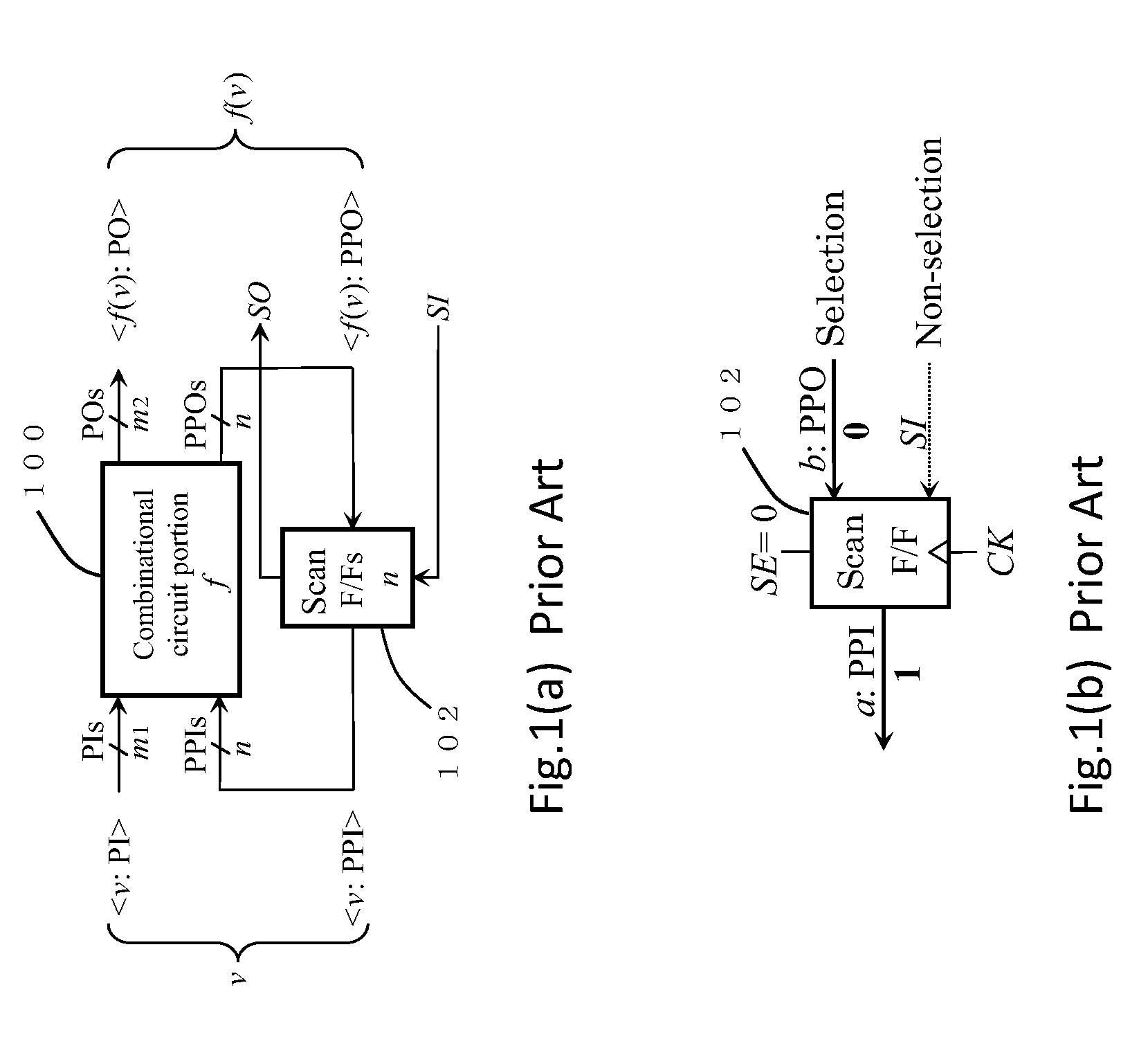
[0057]Referring to FIG. 1, an ordinary full-scan circuit that is a background technique of the present invention will be described.
[0058]FIG. 1(a) is a schematic diagram showing a configuration of an ordinary full-scan circuit. This full-scan circuit is configured to include a combinational circuit portion 100 and scan flip-flops 102 of a full-scan sequential circuit. The combinational circuit portion 100 includes primary input lines (PIs), pseudo primary input lines (PPIs) that are output lines of the scan flip-flops, primary output lines (POs), and pseudo primary output lines (PPOs) that are input lines of the scan flip-flops. Test vectors v input to the combinational circuit portion 100 includes vectors directly applied from the primary input lines and vectors applied via the pseudo primary input lines. The vectors are set to the scan flip-flops 102 by scan shift. Outputs from the combinational circuit p...
PUM
 Abstract
Description
Claims
Application Information