Semiconductor device providing a first electrical conductor and a second electrical conductor in one through hole and method for manufacturing the same

a technology of semiconductor devices and through holes, which is applied in the direction of semiconductor devices, semiconductor/solid-state device details, electrical apparatus, etc., can solve the problems of increasing manufacturing costs, difficult to reduce the chip size, and the above value of space is not realistic as a space, etc., to achieve stable manufacturing, reduce manufacturing costs, and reduce manufacturing costs

Active Publication Date: 2011-06-21
TESSERA ADVANCED TECH
View PDF18 Cites 40 Cited by
  • Summary
  • Abstract
  • Description
  • Claims
  • Application Information

AI Technical Summary

Benefits of technology

[0020]Further, according to the manufacturing methods disclosed in Japanese Patent Laid-Open No. 1998-223,833, Japanese Patent Laid-Open No. 2002-170,904, and Japanese Patent Laid-Open No. 2002-43,502, wider width of the through hole to be filled provides longer filling time when the through hole is filled via a plating technique or a chemical vapor deposition (CVD). In particular in the electrolytic plating technique, the plated metal is easily pinched off at the upper end of the opening to be stuffed up in the case of having larger aspect ratio to generate unwanted voids therein, and therefore it is necessary to add expensive additives to a plating solution and reduce the current density for the plating so as to fill thereof at a lower filling rate. Therefore, only a lower throughput is achieved in the plating process (for example, about 12 hours is required for plating one piece in the case of the diameter of 5 micron and the aspect ratio of 7), and thus the plating process in this case is a process that requires higher costs.
[0035]The method according to the present invention may include a process, in which further comprises forming a multi-layered structure having equal to or more than three layers by repeating the process that is formed the insulating film and the conductive film in this sequence inside the second electrically conductive film after forming the second electrically conductive film. Having such process, a multiplex through electrode having a plurality of electrical conductor formed around a central axis thereof can be stably manufactured.

Problems solved by technology

In addition, in view of the reliability of the device, an active element and / or a passive element such as a transistor cannot be arranged in a certain region just above or in a circumference of the through electrode.
Thus, larger area of the region that cannot arrange any element is provided as larger number of the through electrodes are to be provided, and thus the miniaturization of the chip size is difficult.
Further, when the required number of the signal lines for a power supply, grounding (GND) and a clock is additionally considered, the above value of area is not realistic as a space for disposing the through electrodes in the chip.
Further, although the electrical conductive film on the face is removed via a chemical mechanical polishing (CMP) after completing the plating technique according to the manufacturing method disclosed in Japanese Patent Laid-Open No. 1998-223,833, the performing the CMP technique causes a problem of increasing a manufacturing cost, as slurry is wasted after every wafer is polishing.

Method used


Image

  • Semiconductor device providing a first electrical conductor and a second electrical conductor in one through hole and method for manufacturing the same
  • Semiconductor device providing a first electrical conductor and a second electrical conductor in one through hole and method for manufacturing the same
  • Semiconductor device providing a first electrical conductor and a second electrical conductor in one through hole and method for manufacturing the same

Examples


first embodiment

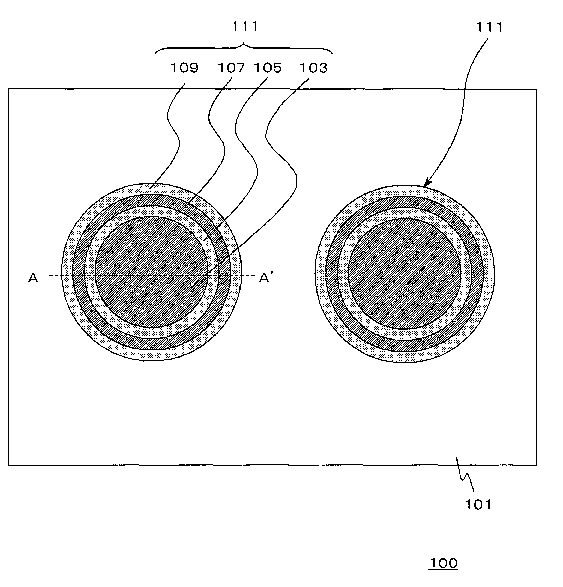
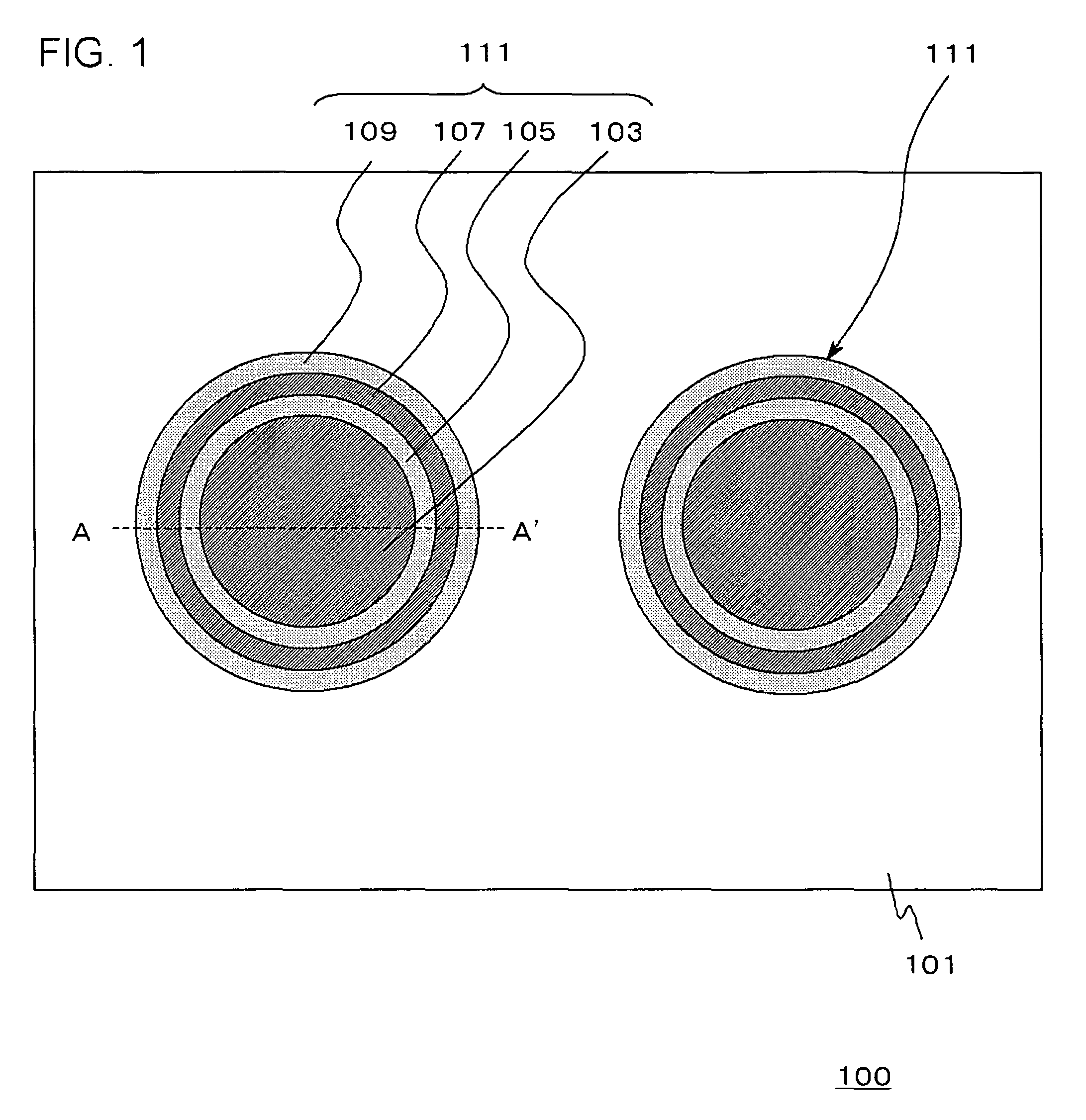
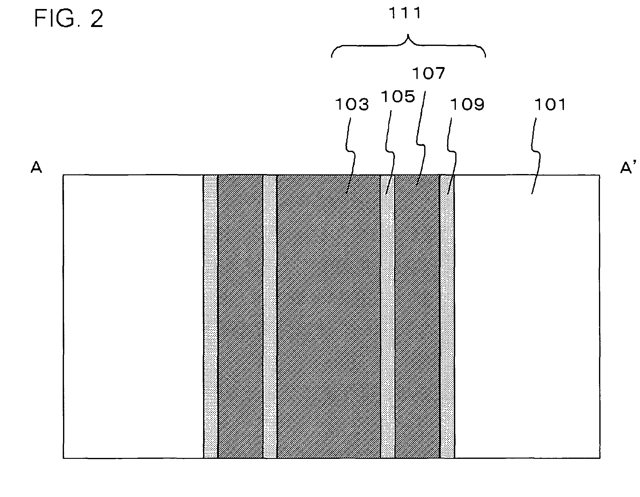
[0062]The present embodiment relates to a semiconductor device provided with duplex through vias extending through the semiconductor substrate. FIG. 1 is a plan view, schematically showing a configuration of a semiconductor device according to the present embodiment. FIG. 2 is a cross-sectional view of FIG. 1 along the line A-A′.

[0063]A semiconductor device 100 shown in FIG. 1 and FIG. 2 includes a silicon substrate 101 and a multiplex through plug 111 that fills an opening that extends through the silicon substrate 101. The multiplex through plugs 111 comprises a columnar and solid first through electrode 103, a cylindrical first insulating film 105 that covers the cylindrical face of the first through electrode 103, a second through electrode 107 that covers the cylindrical face of the first insulating film 105 and a cylindrical second insulating film (outer insulating film) 109 that covers the cylindrical face of the second through electrode 107, and these component have a common...

second embodiment

[0110]The present embodiment relates to an interconnect structure that employs the semiconductor device 100 described in the first embodiment. Firstly, a case that a single sided interconnect is provided will be described. FIG. 7 to FIG. 9 are the cross-sectional views, schematically showing a configuration of a semiconductor device, in which an interconnect is coupled to a multiplex through plug 111. While the configuration of providing one multiplex through plug 111 in the silicon substrate 101 is illustrated in FIG. 7 to FIG. 9, quantity and arrangement of the multiplex through plugs 111 may be suitably selected depending on the design of the device.

[0111]Firstly, a configuration of a semiconductor device shown in FIG. 7 will be described. The semiconductor device shown in FIG. 7 has a configuration, in which a multiplex through plug 111 is coupled to an inter-chip coupling terminal through one layer of an interconnect and is coupled to an inter-chip coupling terminal (a bump jus...

third embodiment

[0122]In the semiconductor device 100 described in the first embodiment, in the multiplex through plug 111 comprising a plurality of through electrodes in bamboo shoot-shaped disposed in a multiplex manner, includes the first through electrode 103 provided in the center of the multiplex through plug 111 that is a solid columnar component. In the present embodiment, a configuration of having a first through electrode 103 that is a pipe-shaped columnar component, center of which is filled with an insulating plug, will be described.

[0123]FIG. 10 is a plan view, schematically showing a configuration of a semiconductor device 110 according to the present embodiment. FIG. 11 is a cross-sectional view of FIG. 10 along B-B′. A semiconductor device 110 shown in FIG. 10 and FIG. 11 has a multiplex through plug 137. A basic configuration of the multiplex through plug 137 is almost similar to the multiplex through plug 111 provided in the semiconductor device 100 shown in FIG. 1, except that a ...


PUM


Abstract

A semiconductor device 100 is provided with a multiplex through plug 111 that fills an opening extending through the silicon substrate 101. The multiplex through plugs 111 comprises a column-shaped and solid first through electrode 103, a first insulating film 105 that covers the cylindrical face of the first through electrode 103, a second through electrode 107 that covers the cylindrical face of the first insulating film 105 and a second insulating film 109 that covers the cylindrical face of the second through electrode 107, and these have a common central axis. The upper cross sections of the first insulating film 105, the second through electrode 107 and the second insulating film 109 are annular-shaped.

Description

[0001]This application is based on Japanese patent application NO. 2004-194,924, the content of which is incorporated hereinto by reference.BACKGROUND OF THE INVENTION[0002]1. Field of the Invention[0003]The present invention relates to a semiconductor device comprising a through electrode and method for manufacturing thereof.[0004]2. Related Art[0005]In recent years, semiconductor chips (hereinafter referred to as simply “chips”) having very large scale integrated circuit (VLSI) are frequently employed for forming critical portions in computers and communication devices. A structure of forming a multi-layered component by forming a plurality of chips or a structure of coupling the chips to the interconnect board via a flip-chip coupling is often employed among the usages of such chips. A technique for providing an electrical conduction between the front side and back side of the chip is critical, in the case that a plurality of chips are employed to form a multi-layered component o...

Claims


Application Information

Patent Timeline
Patent Type & Authority Patents(United States)
IPC IPC(8): H01L23/48
CPCH01L21/76898H01L23/481H01L23/50H01L23/552H01L25/0657H01L25/50H01L2924/3025H01L2224/16145H01L2225/06513H01L2225/06541H01L2924/01077H01L2924/01078H01L2924/3011H01L2223/6622H01L24/05H01L2224/02372H01L2224/02379H01L2224/05001H01L2224/05009H01L2224/05025H01L2224/05124H01L2224/05147H01L2224/05155H01L2224/05166H01L2224/05181H01L2224/05184H01L2224/05548H01L2224/05624H01L2224/05647H01L2224/05655H01L2224/05666H01L2224/05681H01L2224/05684H01L2224/13024H01L2224/13025H01L2224/1403H01L2924/12044H01L2924/00H01L2924/00014
Inventor MATSUI, SATOSHI
Owner TESSERA ADVANCED TECH
Why Eureka
Try Eureka