Method and system for routing of integrated circuit design

a technology of integrated circuits and routing methods, applied in the direction of electric digital data processing, instruments, computing, etc., can solve the problems of inferior wiring quality, negative effect of design performance, inferior wiring quality, etc., and achieve the effect of improving local wiring quality

Inactive Publication Date: 2011-06-21
GLOBALFOUNDRIES INC
View PDF4 Cites 1 Cited by
  • Summary
  • Abstract
  • Description
  • Claims
  • Application Information

AI Technical Summary

Benefits of technology

[0005]It is an object of the invention to provide a method and system for routing electric circuits in integrated chip design in such a way as to improve local wiring quality.

Problems solved by technology

Depending on the quality of placement and of global routing as well as on local wiring requirements, detailed routing often produces local areas with inferior quality of wiring which unnecessarily crowds the wiring channels and has a negative effect on the design's performance.
Such inferior wiring quality includes unconnects (i.e. nets which could not be connected by wiring) as well as so-called scenic routes (i.e. nets which, instead of following minimizing wiring length with long straight segments and few changes of wire level, are composed of many small segments and contain many vias).
This kind of inferior quality wiring usually only occurs in relatively small congested areas.
In addition to diminishing the design's performance, unconnects and scenic routes squander routing resources, contribute to wiring congestion and can cause “hot spots” on the chip which can lead to overload and failure thereof.
The situation is aggravated in the presence of multi-segment nets which underlie a strong requirement to use redundant vias, thus causing additional blockade and making the congestions even worse.
In the past, local wiring improvement was mostly performed manually, requiring a considerable amount of time-consuming interaction by the designer.
If critical parameters were not satisfactory, manual steps 258 were performed, trying to locally “repair” deficient routing results.
In the case of unconnects, manual interaction or retries were necessary, because otherwise the local router was unable to finish all routes.
All such manipulations were carried out on a trial-and-error basis, making them highly time-consuming and tending to result in unacceptable delays in chip development.
Even though some routers comprise “clean steps” features, these were found to often leave the wiring in a worse state than before.

Method used


Image

  • Method and system for routing of integrated circuit design
  • Method and system for routing of integrated circuit design
  • Method and system for routing of integrated circuit design

Examples


Embodiment Construction

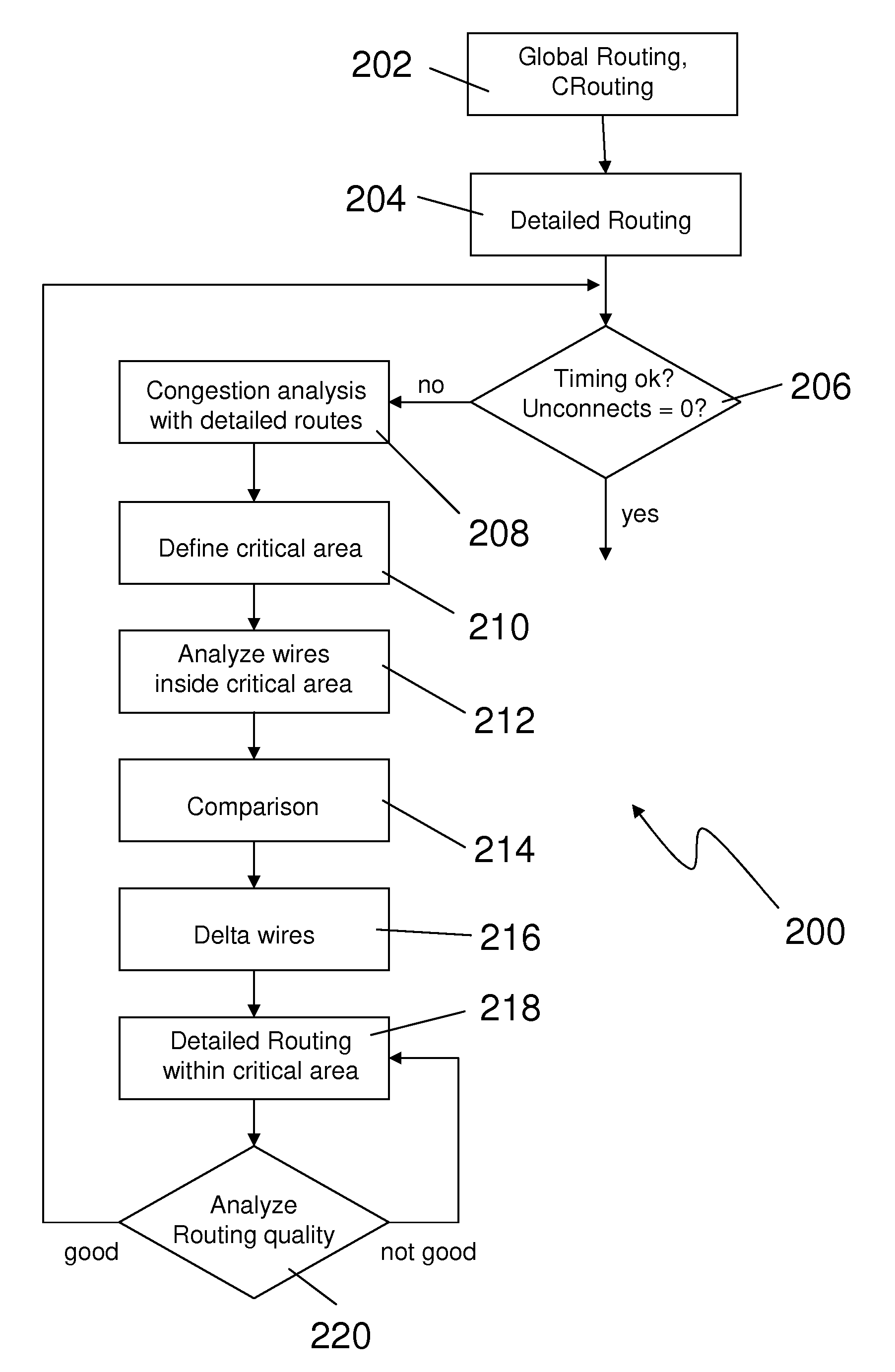
[0019]Generally, the present invention provides a method for rerouting a cell design comprising electric circuits, transistors etc. on a chip in such a way that wiring congestion can be reduced. More specifically, the invention provides a method of improving local wiring quality, especially by straightened wiring in critical areas and replacing inferior quality wiring such as unconnects, scenic routes etc.

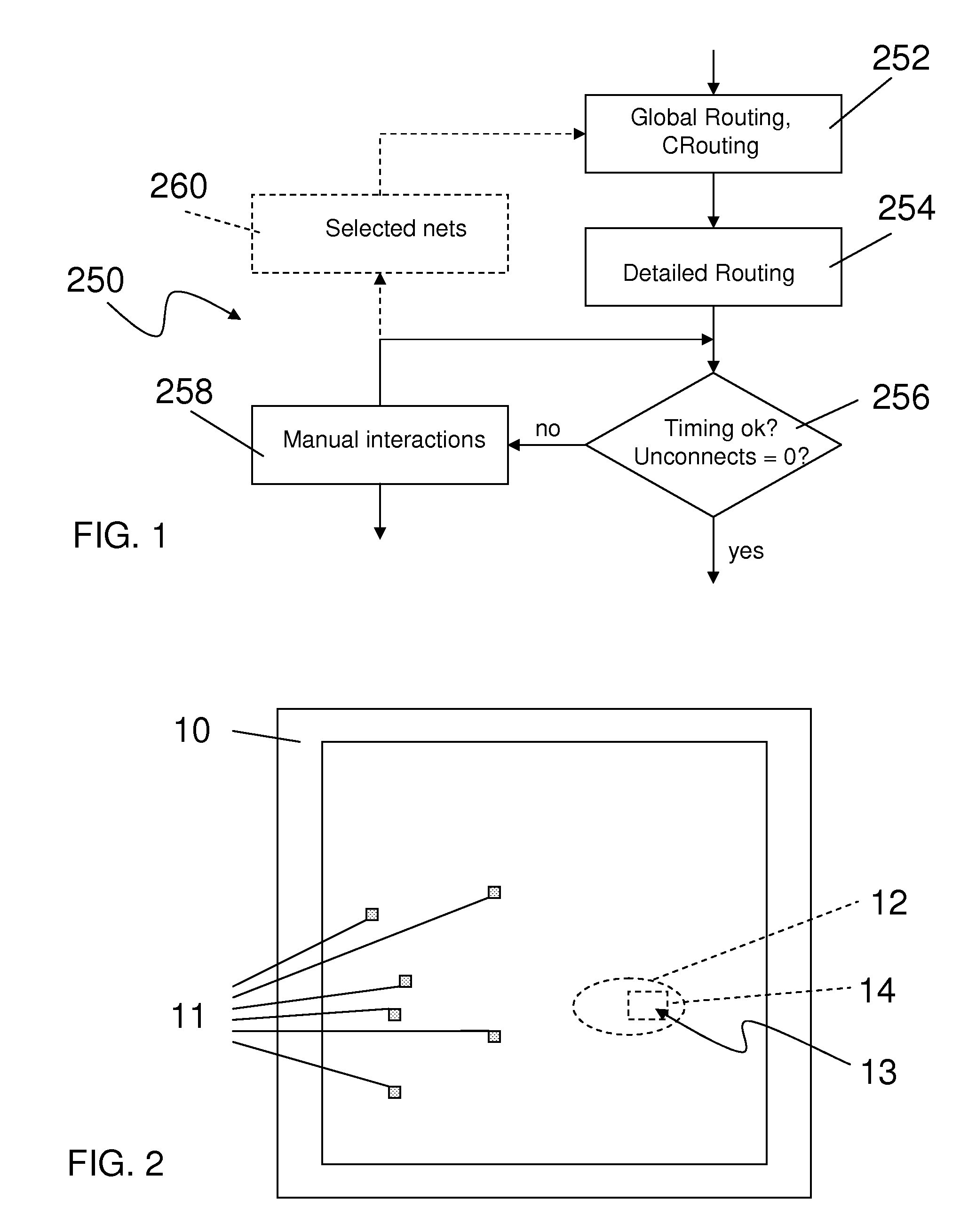
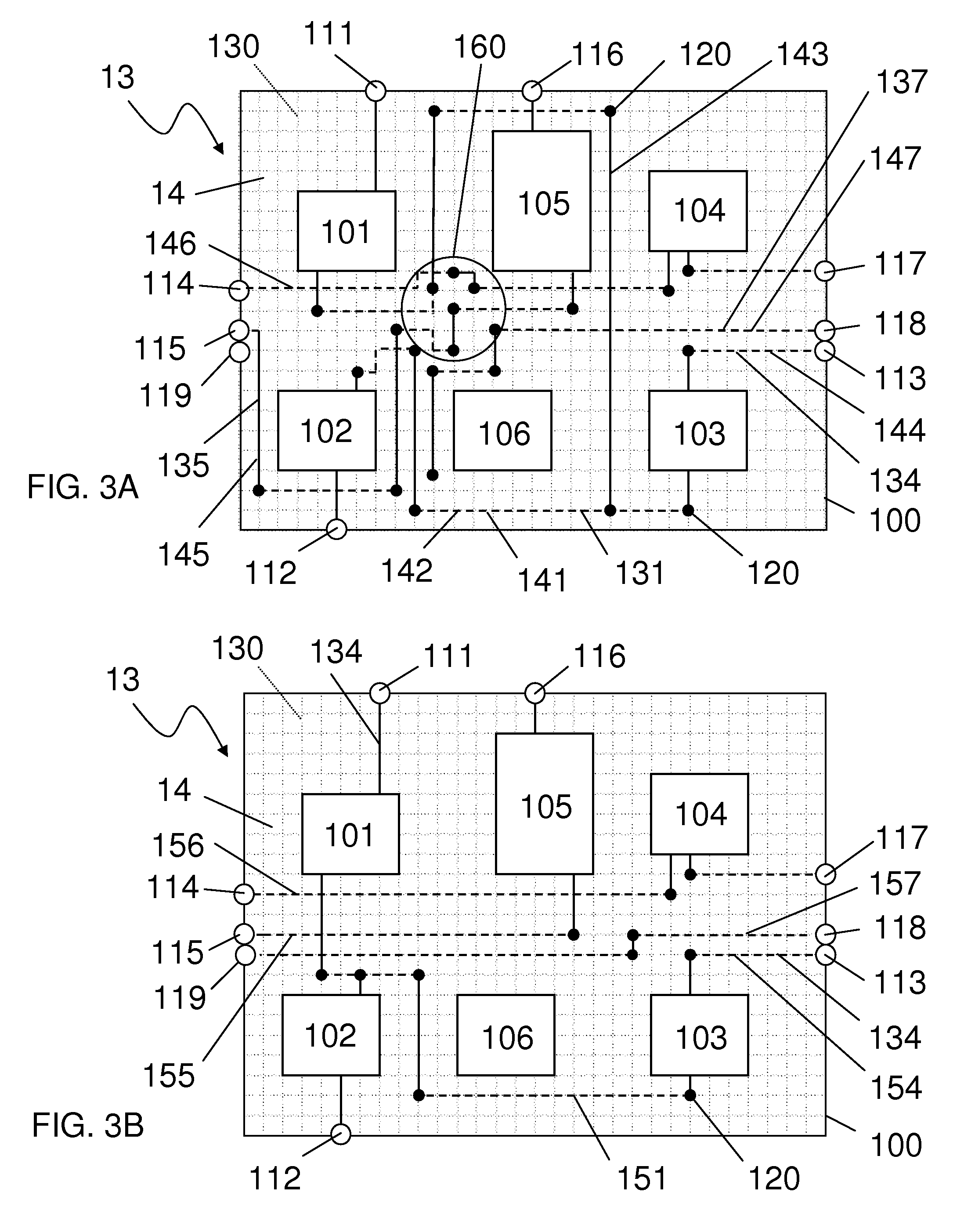
[0020]FIG. 2 shows a schematic view of a chip 10 containing a multitude of cells 11 of which only a tiny fraction is shown in FIG. 2. The process of positioning and arranging the cells on the chip starts out from a netlist which comprises a description of the cells 11 and their connections. A system partitioning step divides a large system into blocks, and a floorplanning step arranges the blocks of the netlist on the chip.

[0021]In a subsequent placement step, the cells 11 are exactly positioned on the chip 10. The objective of the placement step consists in distributing the cells ...


PUM


Abstract

The invention relates to a method and a system for routing electric circuits in integrated circuit chip design. Specifically, the invention encompasses the steps of performing a congestion analysis for a given routed placement of cells containing said electric circuits on a chip; defining a critical area on said chip based on congestion information; analyzing actual wiring quality within said critical area; comparing an actual wiring quality of said critical area with a reference wiring quality of said critical area; and rerouting said critical area based on a comparison between the actual wiring quality and the reference wiring quality.

Description

FIELD OF THE INVENTION[0001]The invention relates to the design of very large scale integrated (VLSI) circuits. Specifically, the invention provides a method and a system for improving routing of electric circuits on a chip in such a way as to decrease local wiring congestion and to enhance wiring resources in congested areas.BACKGROUND OF THE INVENTION[0002]In the manufacture of microelectronics, circuits and other logic must be placed on chips and routed under certain wireability and timing constraints. Specifically, the electric circuits must be placed and routed in such a way that all wiring corresponding to the nets joining the electric circuits can be placed and connected as required. As a rule, routing begins after a floorplan has been laid out and the electric circuits have been placed on the chip. Routing is generally split into a global routing step followed by a detailed routing step. During global routing, a complete set of instructions is provided according to which the...

Claims


Application Information

Patent Timeline
Patent Type & Authority Patents(United States)
IPC IPC(8): G06F17/50
CPCG06F17/5077G06F30/394
Inventor DAELLENBACH, LUKAS
Owner GLOBALFOUNDRIES INC
Why Eureka
Try Eureka