Screening nest, method of screening wiring layers in a multi-layer ceramic and cleaning the screening mask and mask cleaning station

Inactive Publication Date: 2006-07-20
IBM CORP
View PDF1 Cites 1 Cited by
  • Summary
  • Abstract
  • Description
  • Claims
  • Application Information

AI Technical Summary

Benefits of technology

[0010] It is yet another purpose of the invention to extend screening mask life.
[0011] The present invention relates to a screening nest, method of screening green sheets and cleaning the mask and a mask cleaning station. The screening nest includes an electromag

Problems solved by technology

Performance and signal density demands in semiconductor chip packaging are forcing Single Chip Modules (SCMs) and, especially, Multi-Chip Modules (MCMs) to become more and more complex.
Misprinted lines or spaces on a single green sheet may ruin the entire product.
Unfortunately, a poorly (over or under) tensioned mask distorts the screened pattern.
If the mask is over-tensioned, it may stretch out of shape.
Each cleaning causes mask wear, such that the mask m

Method used


Image

  • Screening nest, method of screening wiring layers in a multi-layer ceramic and cleaning the screening mask and mask cleaning station
  • Screening nest, method of screening wiring layers in a multi-layer ceramic and cleaning the screening mask and mask cleaning station
  • Screening nest, method of screening wiring layers in a multi-layer ceramic and cleaning the screening mask and mask cleaning station

Examples


Embodiment Construction

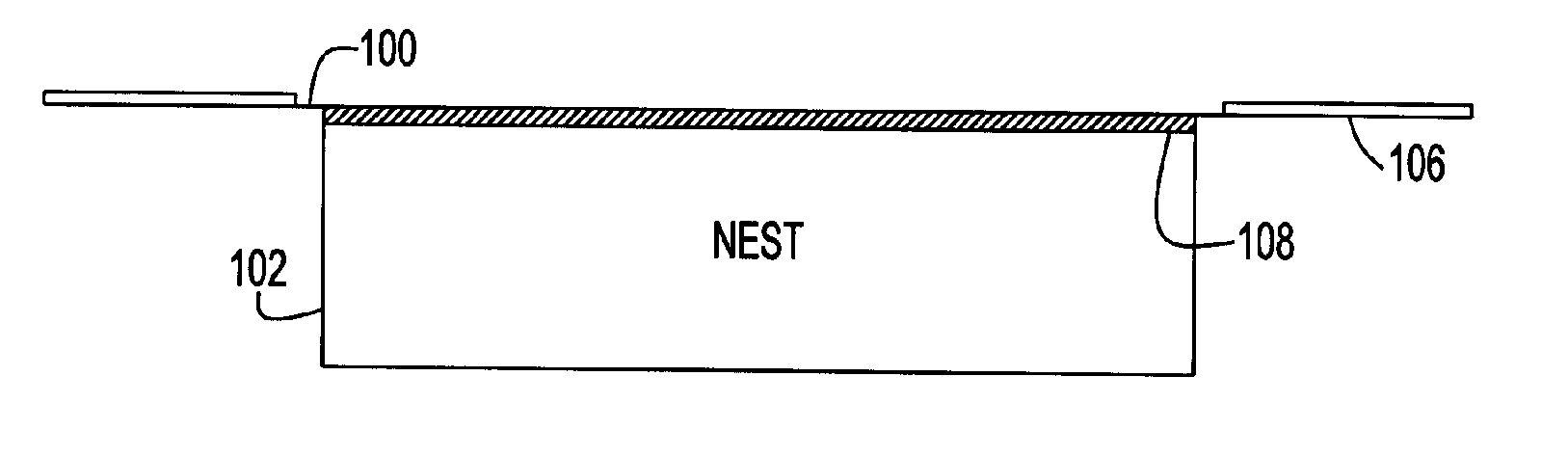
[0019]FIG. 1A shows an example of a preferred embodiment mask 100 and nest 102 arrangement according to the present invention. Primarily, the mask 100 is of a magnetic or ferromagnetic material (e.g., nickel) and the nest 102 includes a switchable magnetic field, e.g., one or more electromagnet embedded in the nest 102. As is typical of metal masks used in printing green sheets, the preferred mask 100 is an electroformed metal mask of a patterned copper core electroplated with nickel and held in any suitable frame 106, preferably of non-magnetic material. A green sheet 108 is located on the upper surface of the nest 102. The copper core does not exhibit magnetic properties while the ferromagnetic plating material (nickel) can be temporarily magnetized in a magnetic or an electromagnetic field. Thus, by activating the electromagnet the mask 100 is magnetically clamped to the green sheet 108 during screening for a high quality image; and thereafter, quickly and cleanly magnetically se...


PUM


Abstract

A screening nest, method of screening green sheets and cleaning the mask and a mask cleaning station. The screening nest includes an electromagnet that clamps the mask to a green sheet on the nest during screening. The mask may be electromagnetically dampened during application and removal. The cleaning station electromagnetically dampens the mask during cleaning and especially during rinsing and drying.

Description

BACKGROUND OF THE INVENTION [0001] 1. Field of the Invention [0002] The present invention is related to integrated circuit (IC) chip packaging and more particularly to a screening station for screening paste onto a ceramic green sheet and to a station for cleaning the screening mask between screenings. [0003] 2. Background Description [0004] Performance and signal density demands in semiconductor chip packaging are forcing Single Chip Modules (SCMs) and, especially, Multi-Chip Modules (MCMs) to become more and more complex. Ceramic module signal density is being increased both by increasing the number of ceramic wiring layers (with one wiring or power layer on each ceramic layer) and by printing narrower and narrower lines on finer and finer pitch. Wiring is printed on an uncured ceramic substrate layer (green sheet), e.g., using a metal mask and screening a paste (molybdenum paste, copper paste, copper / glass paste) pattern onto green sheets to define wiring lines and spaces. Such p...

Claims


Application Information

Patent Timeline
IPC IPC(8): B08B3/00B05D5/00
CPCB08B3/022H01L21/4867H05K1/0306H05K3/1216H05K3/26H05K2203/0165H05K2203/104
Inventor HARMUTH, JOHN F.HERRON, LESTER W.SEMKOW, KRYSTYNA W.
Owner IBM CORP
Why Eureka
Try Eureka