Differential sensing and TSV timing control scheme for 3D-IC

a technology of tsv timing control and differential sensing, which is applied in the direction of logic circuit coupling/interface arrangement, pulse technique, instruments, etc., can solve the problems of critical affecting the speed and efficiency of the sram, contributing significantly to the overall power consumption of the sram, and increasing the overall operating speed of the memory devi

Active Publication Date: 2011-06-28
NATIONAL TSING HUA UNIVERSITY
View PDF8 Cites 197 Cited by
  • Summary
  • Abstract
  • Description
  • Claims
  • Application Information

AI Technical Summary

Benefits of technology

[0010]An aspect of the present invention is to provide a method and a scheme for 3D-IC Differential Sensing and TSV timing control.
[0011]The differential sensing and TSV timing control for 3D-IC comprises a relative high ability driver (buffer); a dummy loading coupled to the relative high ability driver to transmit a timing strobe signal; a detecting circuit coupled to the dummy loading. A differential signal generating structure is coupled to a relative low ability driver (buffer) to generate a differential signal. A sensing circuit is coupled to the differential signal generating structure. The detecting circuit activates the sensing circuit when an active signal reaches to a trigger point.
[0012]The differential signal generating structure includes a pair of high loading structures coupled to the relative low ability driver; an inverter arranged between one of the pair of high loading structures and the relative low ability driver. The pair of high loading structures includes a pair of through-silicon-vias. The dummy loading structure includes a through-silicon-via.
[0013]The signal transmitting speed of the relative high ability driver is higher than the one of the relative low ability driver. In one embodiment, the signal transmitting speed of the relative high ability driver is x-times to the relative low ability driver. The detecting circuit includes at least one inverter, and the sensing circuit includes a sense amplify or comparator or operational amplifier.
[0014]Under the scheme of three dimension aspect, the differential sensing and TSV timing control scheme for a stacked device having pluralities chip layers includes a first chip layer having a detecting circuits and a relative high ability drive horizontally coupled to the detecting circuits. A sensing circuit is coupled to the detecting circuits by a horizontal conductive line and a first differential signal driver coupled to the sensing circuit, horizontally. A Nth chip layer of the stacked device includes a Nth relative high ability driver and a Nth differential signal driver formed on the Nth chip layer; wherein the N is a nature number and is more than one; wherein the Nth relative high ability drive is vertically coupled to the first relative high ability drive through one relative low loading TSV and (N−2) relative high loading TSV to act dummy loadings, all of the relative low loading TSV and (N−2) relative high loading TSV penetrate the stacked device from the Nth chip layer to the first chip layer, wherein the relative low loading TSV and the (N−2) relative high loading TSVs are formed in a shared configuration; wherein the Nth differential signal driver is vertically coupled to the first differential signal driver through a pair of relative low loading TSVs and (N−2) pairs of relative high loading TSVs, vertically, each pair of relative low loading TSVs and the (N−2) relative high loading TSVs penetrates the stacked device from top to bottom; and each the relative low loading TSV is formed between a first and a second chip layers, and each the relative high loading TSV is formed between any adjacent two chip layers of the stacked device; whereby the detecting circuit activates the sensing circuit when an active signal reaches to a trigger point.

Problems solved by technology

However, the timing of its internal circuitry may critically affect the speed and efficiency of the SRAM.
For example, the bit line pre-charge interval comprises an appreciable portion of the read / write cycle time, and sense amplifier usage contributes significantly to the overall power consumption of the SRAM.
This potentially increases the overall operating speed of the memory device.
The delay caused by the loading issue is worse to the higher level chip layers.

Method used


Image

  • Differential sensing and TSV timing control scheme for 3D-IC
  • Differential sensing and TSV timing control scheme for 3D-IC
  • Differential sensing and TSV timing control scheme for 3D-IC

Examples


Embodiment Construction

[0019]Some sample embodiments of the invention will now be described in greater detail. Nevertheless, it should be recognized that the present invention can be practiced in a wide range of other embodiments besides those explicitly described, and the scope of the present invention is expressly not limited expect as specified in the accompanying claims.

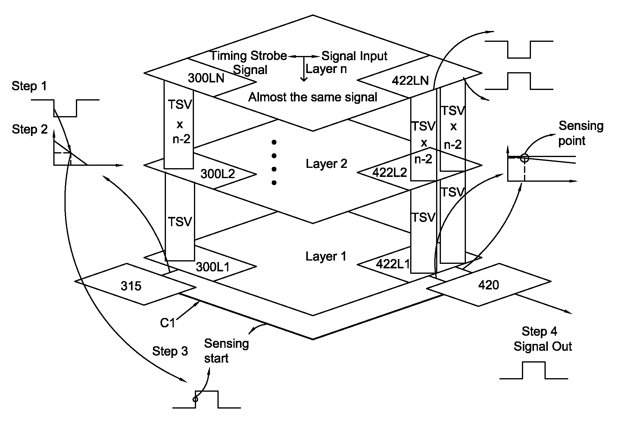
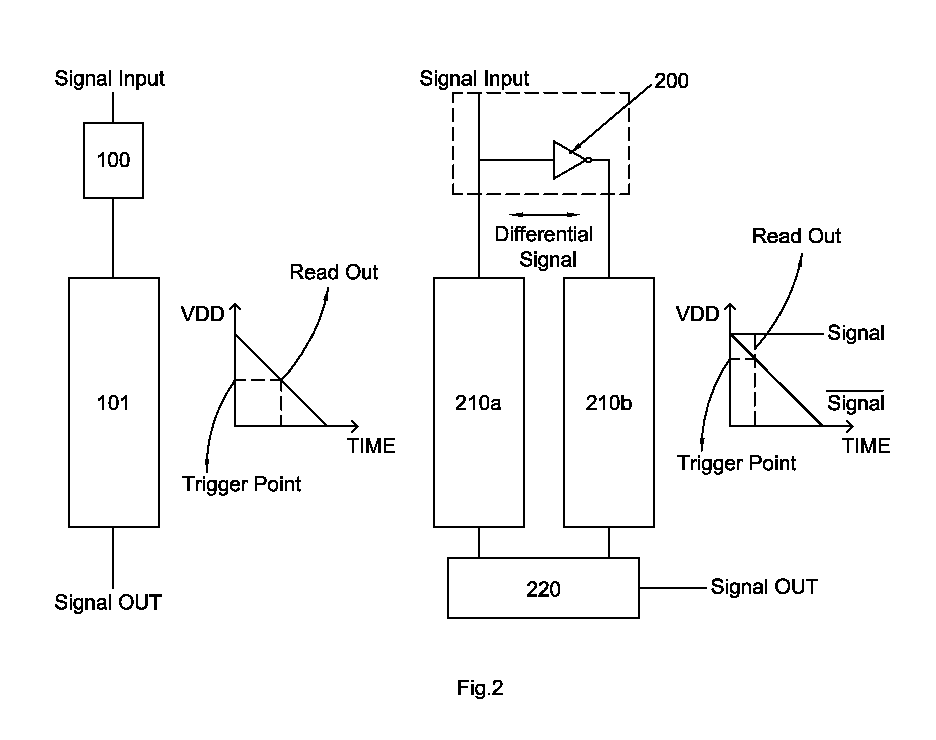
[0020]The present invention generally relates to a 3D-IC differential sensing and TSV timing control scheme which can be introduced to an embedded volatile or nonvolatile memory. In a preferred embodiment of the present invention, as shown in FIG. 2, the present invention discloses a differential sensing scheme which includes a drive or buffer 100 coupled to a first high loading structure 101.

[0021]A signal input is coupled to another terminal of the drive (buffer) 100, a signal output is electrically connected to the first high loading structure which can be formed by TSV 101. The scheme further includes a second high loading structur...


PUM


Abstract

This disclosure uses a differential sensing and TSV timing control scheme for 3D-IC, which includes a first chip layer of the stacked device having a detecting circuits and a relative high ability driver horizontally coupled to the detecting circuits. A sensing circuit is coupled to the detecting circuits by a horizontal line, a first differential signal driver is coupled to the sensing circuit, horizontally. The Nth chip layer of the stacked device includes a Nth relative high ability driver and a Nth differential signal driver formed on the Nth chip layer. The Nth relative high ability driver is vertically coupled to the first relative high ability driver through one relative low loading TSV and (N−2) TSVs to act as dummy loadings. The TSV and (N−2) TSVs penetrate the stacked device from Nth chip layer to first chip layer. The TSV shares same configuration with the (N−2) TSVs. The Nth differential signal driver is vertically coupled to the first differential signal driver through a pair of TSVs and (N−2) pairs of TSVs, vertically. The pair of TSVs and the (N−2) TSVs penetrate the stacked device from the Nth chip layer to the first chip layer. Each of TSV is formed between a first and a second chip layers. Each of TSV is formed between any adjacent two chip layers of the stacked device.

Description

TECHNICAL FIELD[0001]The present invention generally relates to a 3D stacked chip device, and especially to a differential sensing and TSV timing control scheme for 3D-IC.RELATED ART[0002]Recently, portable electronic equipment such as mobile telephones and non-volatile semiconductor memory media such as IC memory cards have been downsized, and there have been increasing demands for reducing the number of parts used in the equipment and media and downsizing thereof. Therefore, in the semiconductor industry, packaging technologies for integrated circuits (ICs) have been advancing to meet requirements for miniaturization and mounting reliability. For example, the requirement for miniaturization results in acceleration of technological development for a package having a similar size in relation to a semiconductor chip. Further, the requirement for mounting reliability places importance on packaging technologies that are capable of enhancing efficiency of a mounting process and improvin...

Claims


Application Information

Patent Timeline
Patent Type & Authority Patents(United States)
IPC IPC(8): H03K19/0175
CPCH01L25/0657H03K19/0175H01L2225/06541H01L2924/0002H01L2924/00
Inventor WU, WEI-CHENGCHEN, YEN-HUEICHANG, MENG-FAN
Owner NATIONAL TSING HUA UNIVERSITY
Why Eureka
Try Eureka