SPI bank addressing scheme for memory densities above 128Mb

a technology of addressing scheme and memory, applied in the field of peripheral interface devices, can solve the problems of reducing speed, increasing cost, and reducing data storage density, so as to achieve the effect of not having to undergo costly and time-consuming redesign

Active Publication Date: 2011-07-12
MONTEREY RES LLC
View PDF6 Cites 6 Cited by
  • Summary
  • Abstract
  • Description
  • Claims
  • Application Information

AI Technical Summary

Benefits of technology

[0016]In addition, the system and method of the present invention is applicable to and reliable for various memory technologies.
[0026]The present invention thereby provides a method of addressing larger arrays (e.g., >128 Mb) of flash memory cells using current and legacy based SPI-processor devices that allow backward compatibility without costly and time consuming redesign.

Problems solved by technology

For example, DRAM and SRAM allow individual-bits of data to be erased one at a time, but such memory loses its data when power is removed.
EEPROM can alternatively be easily erased without extra exterior equipment, but has reduced data storage density, lower speed, and higher cost.
EPROM, in contrast, is less expensive and has greater density but lacks ease of erasability.
In addition, ever increasing numbers of peripheral devices also demand attention of the processor to which they are attached.
However, as such peripheral needs and memory sizes continue to grow, the addressing requirements of current SPI devices will also tend to grow beyond the current 3-byte addressing scheme which limits memory addressing capability to 128 Mb.
Although new SPI-processor chip-sets could be designed that overcome these 3-byte addressing limitations, such system redesigns could be costly and time consuming and may not allow the use of current and legacy devices.

Method used


Image

  • SPI bank addressing scheme for memory densities above 128Mb
  • SPI bank addressing scheme for memory densities above 128Mb
  • SPI bank addressing scheme for memory densities above 128Mb

Examples


Embodiment Construction

[0034]One or more aspects of the present invention are described with reference to the drawings, wherein like reference numerals are generally utilized to refer to like elements throughout, and wherein the various structures are not necessarily drawn to scale. In the following description, for purposes of explanation, numerous specific details are set forth in order to provide a thorough understanding of one or more aspects of the present invention. It may be evident, however, to one skilled in the art that one or more aspects of the present invention may be practiced with a lesser degree of these specific details. In other instances, well-known structures and devices are shown in block diagram form in order to facilitate describing one or more aspects of the present invention.

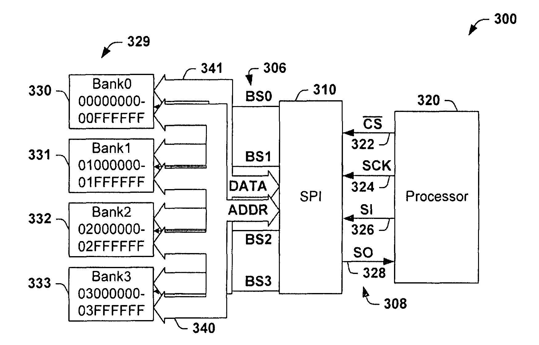
[0035]Improvements in the density of memory devices translate to increased memory capacity. Density and thus capacity is a major consideration in the cost of fabrication and the marketability of memory devices...


PUM


Abstract

Systems and methods of addressing two or more banks of memory utilizing a single-bank serial peripheral interface and an at least three-byte address protocol are provided. In one embodiment, a serial peripheral interface comprises a serial processing component configured to address one of the memory banks using the three-byte addressing scheme, and to write data to or read data from the addressed bank, and a bank register pointer component coupled to the serial processing component, the pointer component comprising two or more bank register pointers associated with respective memory banks, and configured to select one of the memory banks based on the two or more bank register pointers, wherein the bank register pointer component selects one of the two or more memory banks, and the serial processing component writes data to or reads data from the selected bank of memory according to the three-byte addressing scheme.

Description

FIELD OF INVENTION[0001]The present invention relates generally to peripheral interface devices and the like, and in particular, to a system and method of addressing two or more banks of memory utilizing a single-bank serial peripheral interface device and a three-byte addressing protocol.BACKGROUND OF THE INVENTION[0002]Many different types and styles of memory exist to store data for computers and similar type systems. For example, random access memory (RAM), dynamic random access memory (DRAM), static random access memory (SRAM), read only memory (ROM), programmable read only memory (PROM), electrically programmable read only memory (E-PROM), electrically erasable programmable read only memory (EEPROM) and flash memory are all presently available to accommodate data storage.[0003]Each type of memory has its own particular advantages and disadvantages. For example, DRAM and SRAM allow individual-bits of data to be erased one at a time, but such memory loses its data when power is ...

Claims


Application Information

Patent Timeline
Patent Type & Authority Patents(United States)
IPC IPC(8): G06F13/28
CPCG06F12/06G06F2212/1004G06F2212/2022
Inventor LE, ANTHONYKITCHEN, MALCOLMHUANG, JACKSON
Owner MONTEREY RES LLC
Why Eureka
Try Eureka