Electromagnetic band-gap structure

a technology of electromagnetic band and structure, applied in the direction of structural forms of radiation elements, electrical equipment, simultaneous aerial operations, etc., can solve the problems of heavy structure and bulky structure, and achieve the effect of uniform structure and simplified manufactur

US7982673B2Inactive Publication Date: 2011-07-19BAE SYSTEMS PLC
11 Cites 28 Cited by

Patent Information

Authority / Receiving Office
US · United States
Patent Type
Patents(United States)
Current Assignee / Owner
Publication Date
2011-07-19
Estimated Expiration
Not applicable · inactive patent

Smart Images

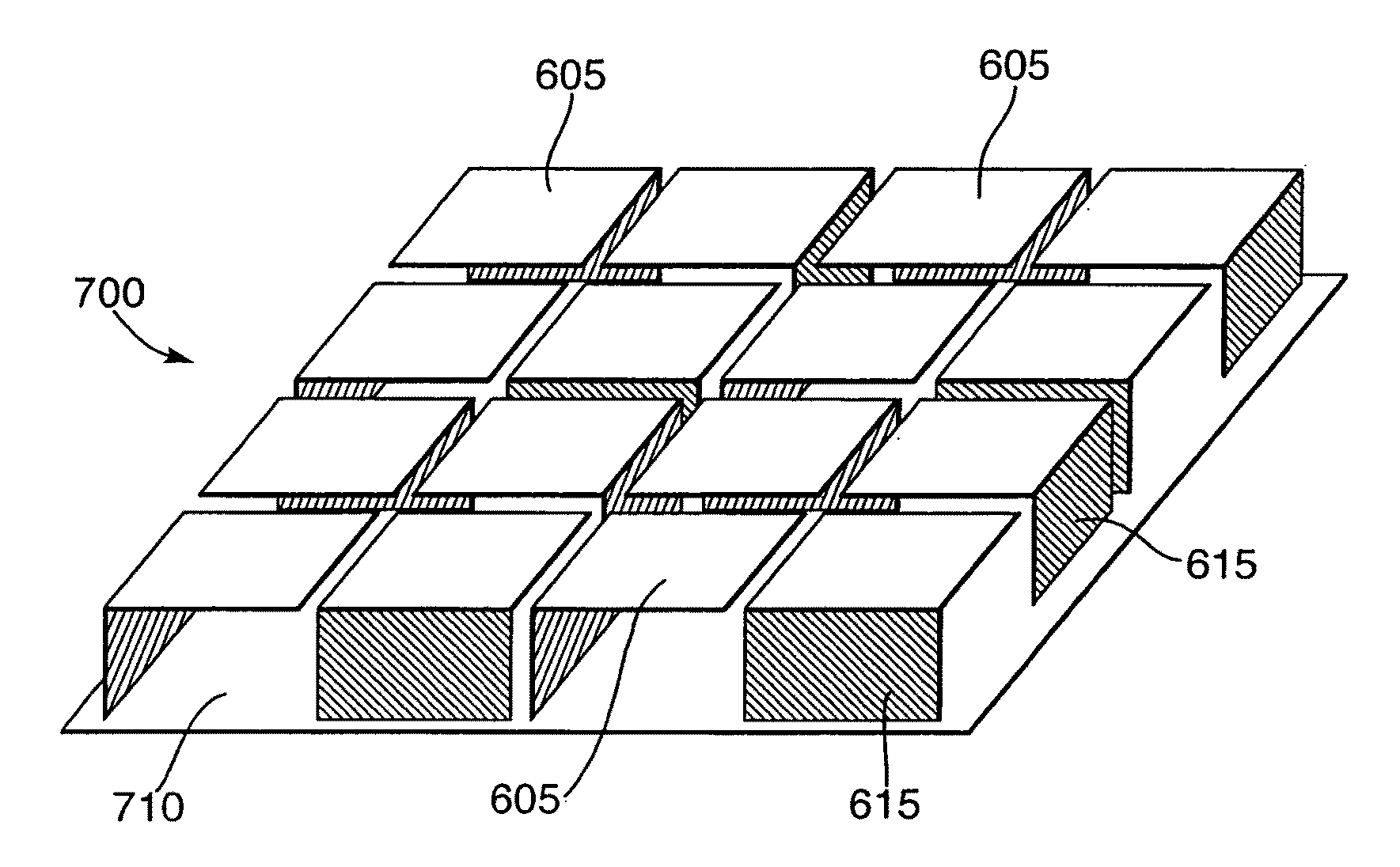
  • Figure 1
    Figure 1
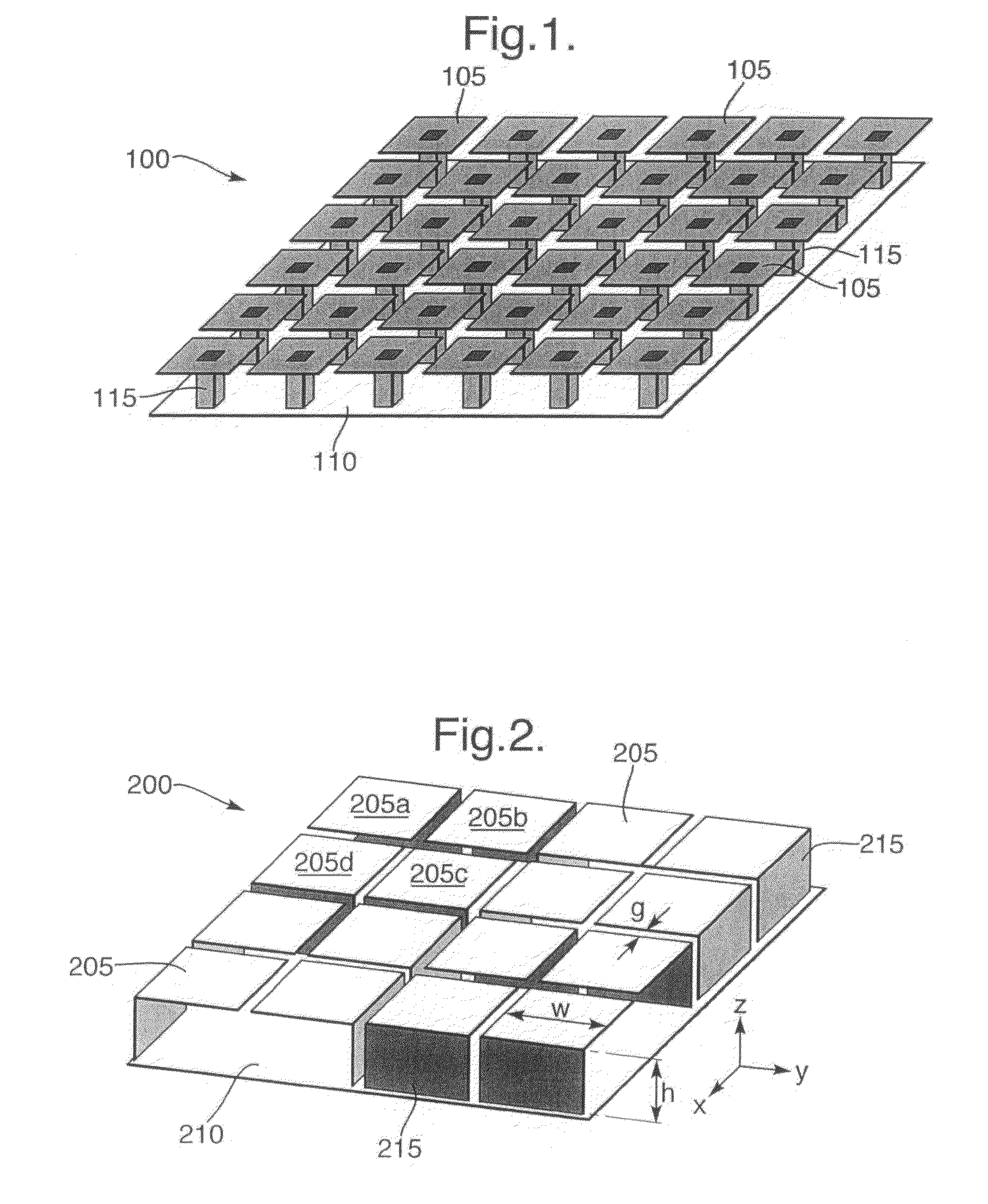
  • Figure 2
    Figure 2
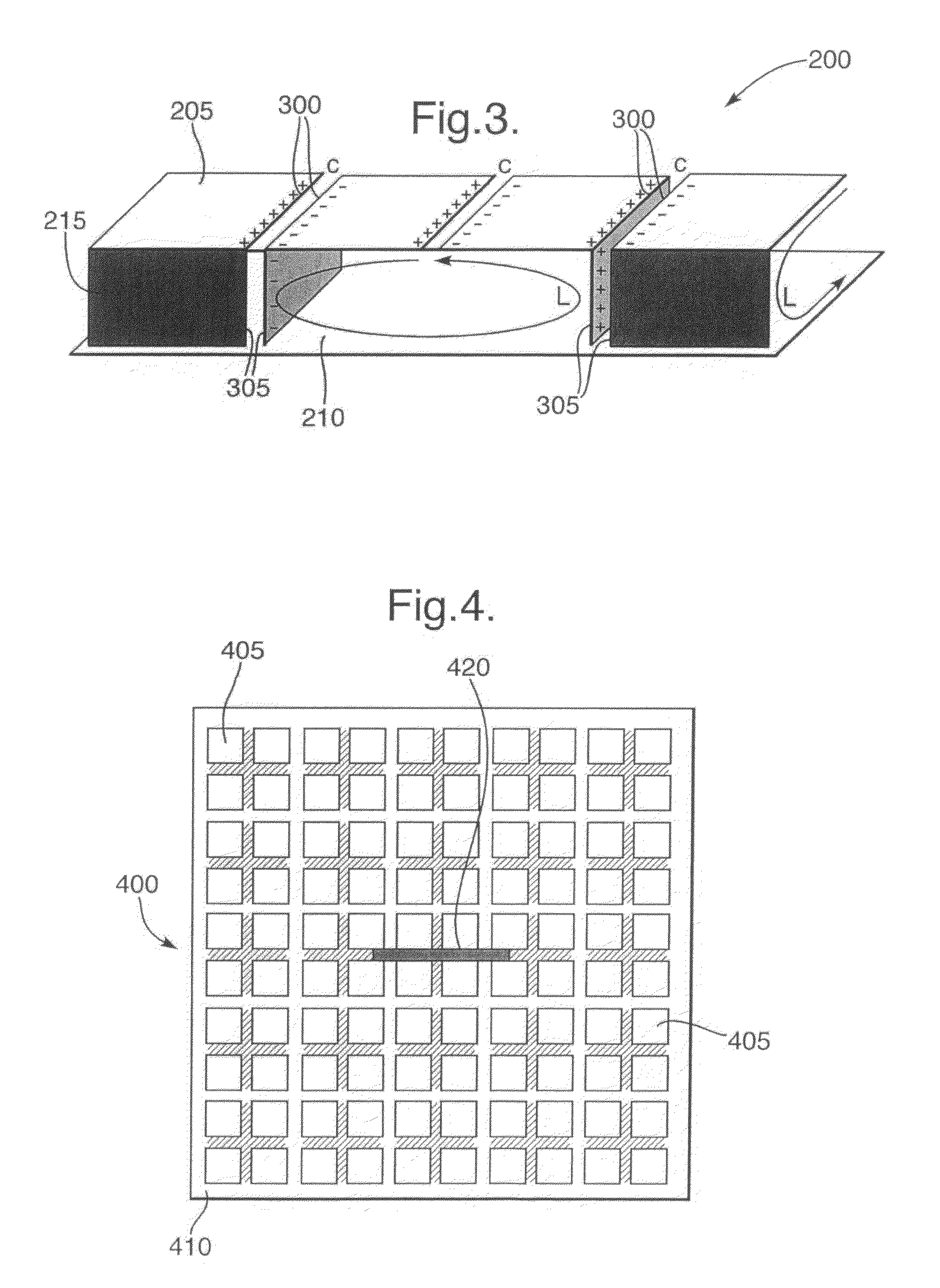
  • Figure 3
    Figure 3
Patent Text Reader

Abstract

An electromagnetic band gap structure is provided including a ground plane and a periodic planar arrangement of surface elements mounted parallel to and at a predetermined distance from the ground plane. Each of the surface elements is supported in the planar arrangement by at least one conducting support element extending from an edge of the surface element to the ground plane, avoiding back-to-back parallel support elements. This arrangement allows for the surface elements and their respective support elements to be folded from flat metal templates to greatly simplify manufacture. An antenna is also provided in which an antenna element is mounted in such a way as to use the electromagnetic band-gap structure as a ground plane. This allows for a low-profile antenna to be made as the antenna element may be mounted close to the plane of surface elements in the structure.
Need to check novelty before this filing date? Find Prior Art

Description

RELATED APPLICATION INFORMATION

[0001] This application is a United States National Phase Patent Application of, and claims the benefit of, International Patent Application No. PCT / GB2007 / 050481 which was filed on Aug. 10, 2007, and which claims priority to British Patent Application No. 06270081.0, which was filed on Aug. 18, 2006, and which claims priority to European Patent Application No. 0616391.9, which was filed on Aug. 18, 2006, the disclosures of all of which are incorporated herein by reference.FIELD OF THE INVENTION

[0002] The present invention relates to electromagnetic band-gap structures and in particular, but not exclusively, to an improved structure operable as a high impedance surface for use in low-profile antenna applications operating with electromagnetic radiation in the frequency range 100 MHz to 1 GHz.BACKGROUND INFORMATION

[0003] In an arrangement, discussed for example by D. Sievenpiper, L. Zhang, R. F. J. Broas, N. G. Alexopolous and E. Yablonovitch in “High-Impe...

Examples

Embodiment Construction

[0029]Exemplary embodiments of the present invention will now be described in more detail, by way of example only, with reference to the accompanying drawings.

[0030]Electromagnetic band-gap (EBG) structures according to exemplary embodiments of the present invention have been designed to provide a high-impedance surface to electromagnetic radiation at selected frequencies in the range 100 MHz to 1 GHz in particular. These EBG structures are particularly suited for application to low-profile antennae in which they are used to provide a ground plane. At frequencies in the range 100 MHz to 1 GHz, known high-impedance surfaces require large and heavy structures. However, exemplary embodiments of the present invention aim to provide a light-weight structure and one that is simple and inexpensive to make.

[0031]An EBG structure according to an exemplary embodiment of the present invention will now be described with reference to FIG. 2.

[0032]Referring to FIG. 2, a perspective view of a port...