Solid-state imaging device

a solid-state imaging and imaging device technology, applied in the direction of optical elements, instruments, television systems, etc., can solve the problems of preventing the generation of color drift and color mixing, and the silica surface of the light-receiving portion and the color filter may be extremely close to each other, so as to prevent the generation of color drift and color mixing, and the degree of freedom in the optical filter design can be extensively extended

Active Publication Date: 2011-07-26
SONY SEMICON SOLUTIONS CORP
View PDF26 Cites 179 Cited by
  • Summary
  • Abstract
  • Description
  • Claims
  • Application Information

AI Technical Summary

Benefits of technology

[0024]Therefore, a disadvantage that may occur in the case where the silicon surface of the light-receiving portion and the color filter come extremely close to each other may be substantially prevented.
[0046]Furthermore, the use of the quantum dot structure allows an optical filter layer to be configured solid as described above because only a single material system may be used in the manufacture of plural kinds of optical filters having different optical characteristics, such as color filters of the respective colors. In addition, the use of the quantum dot structure allows characteristics of the optical filter layer to be sequentially changed by controlling the diameters of quantum dots. Accordingly, the degree of freedom in the optical filter design can be extensively extended, compared with the optical filter of the related art. That is, the optical characteristics of the typical optical filter have been determined by the inherent optical characteristics of a filter material (e.g., dye or pigment in resist).

Problems solved by technology

Therefore, a disadvantage that may occur in the case where the silicon surface of the light-receiving portion and the color filter come extremely close to each other may be substantially prevented.

Method used


Image

  • Solid-state imaging device
  • Solid-state imaging device
  • Solid-state imaging device

Examples


Embodiment Construction

[0063]First, prior to the description of the preferred embodiment of the present invention, the outline of the present invention will be described.

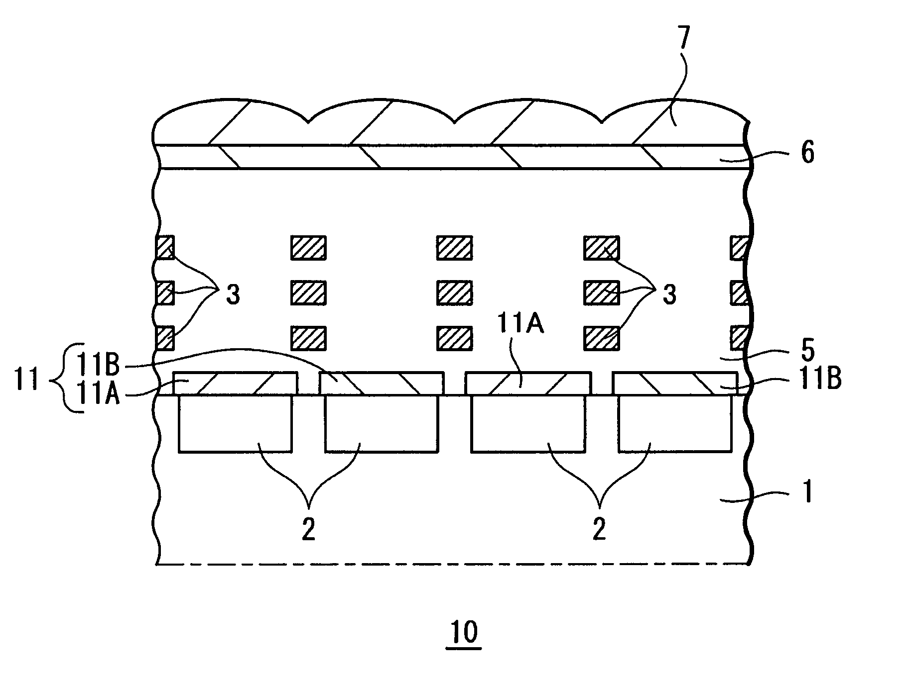
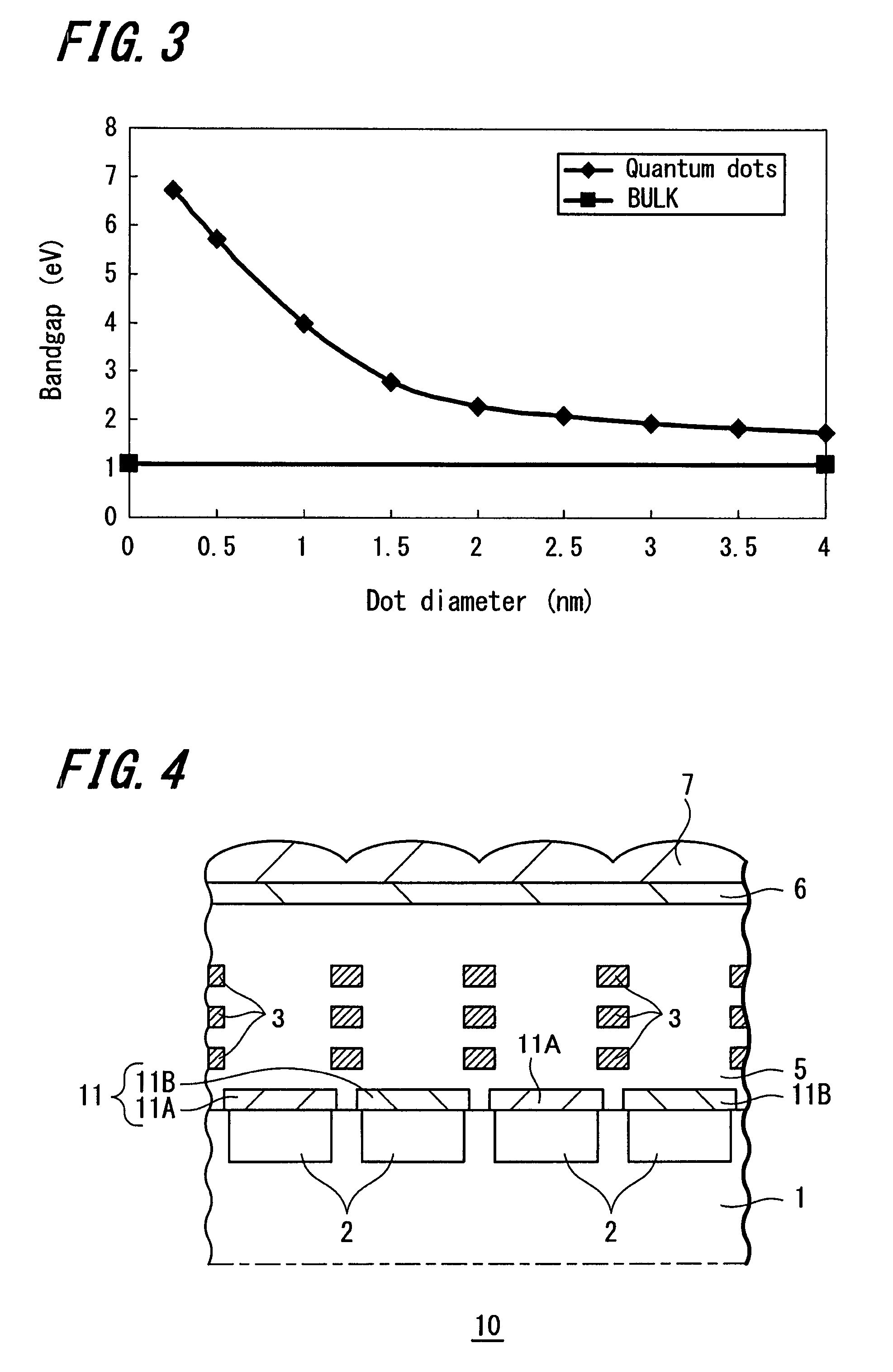
[0064]According to an embodiment of the present invention, a solid-state imaging device includes an optical filter layer directly formed on or formed through another layer (e.g., an insulating layer or a low-reflecting coating) on the surface of the semiconductor substrate in which a light-receiving portion is formed. Here, quantum dots having substantially equal diameters are formed in a layer.

[0065]The quantum dots used may be, for example, silicon dots.

[0066]The layer in which quantum dots are formed is preferably a layer having insulation properties and a lower refractive index than the refractive indexes of the quantum dots. The layer may be, for example, a SiO2 layer or a Si3N4 layer.

[0067]With respect to the silicon dots, researchers have conducted experiments mainly in the field of experimental memory systems (see, for example, Y....


PUM


Abstract

A solid-state imaging device includes a light-receiving portion, an optical filter layer, and quantum dots. The light receiving portion, where a photoelectric conversion is carried out, is formed in a semiconductor substrate. The optical filter layer is directly formed on or formed through another layer on the surface of the semiconductor substrate in which the light-receiving portion is formed. Quantum dots having substantially equal diameters are formed in the optical filter layer. The quantum dots have higher refractive indexes than the refractive index of the optical filter layer in which the quantum dots are embedded.

Description

CROSS REFERENCES TO RELATED APPLICATIONS[0001]The present invention contains subject matter related to Japanese Patent Application JP 2006-287775 filed in the Japanese Patent Office on Oct. 23, 2006 and Japanese Patent Application JP 2007-249966 filed in the Japanese Patent Office on Sep. 26, 2007, the entire contents of which being incorporated herein by reference.BACKGROUND OF THE INVENTION[0002]1. Field of the Invention[0003]The present invention relates to a solid-state imaging device, such as a CMOS solid-state imaging device. In particular, the present invention relates to a color solid-state imaging device using a color filter.[0004]2. Description of the Related Art[0005]In a solid-state imaging device used in an image sensor or the like, incident light can be collected into a light-receiving portion formed of photodiodes of respective pixels and then photo-electrically converted into signals.[0006]The light-receiving portion formed of photodiodes has sensitivities at the wav...

Claims


Application Information

Patent Timeline
Patent Type & Authority Patents(United States)
IPC IPC(8): H01L31/0232G02B5/20G02B5/22H01L27/14H01L31/10H04N5/335H04N5/369H04N5/374
CPCG02B5/201G02B5/223H01L27/14621H01L31/0352H01L27/14645H01L27/14685H01L27/14627
Inventor RENNIE, JOHN
Owner SONY SEMICON SOLUTIONS CORP
Why Eureka
Try Eureka