Incorporation of functionalizing molecules in nanopatterned epitaxial graphene electronics

a functionalizing molecule and graphene technology, applied in semiconductor devices, thin material processing, textiles and paper, etc., can solve the problems the ultimate limit of silicon-based electronics in the near future, and the disadvantages of carbon nanotube-based molecular electronics, etc., to achieve the effect of greatly reducing or eliminating power dissipation at the contacts

Active Publication Date: 2011-08-02
GEORGIA TECH RES CORP
View PDF12 Cites 5 Cited by
  • Summary
  • Abstract
  • Description
  • Claims
  • Application Information

AI Technical Summary

Benefits of technology

[0025]Integrated electronics based on ultra-thin graphite film (UTGF) have several advantages over prior art, these include: large-scale integration is possible using standard microelectronics lithography methods; metals are not used to interconnect the devices so that metal-to-graphite contact resistances are avoided and power dissipation at the contacts is greatly reduced or eliminated; integrated electronic device structures whose operation relies on quantum interference effects can be constructed; feature sizes as small as 1 nm scale are possible and limited only by the lithography methods; and graphite can be electronically modified by chemically bonding molecules to the edges of graphite strips, without damaging the graphitic structure.

Problems solved by technology

However, miniaturization of silicon-based electronics will reach an ultimate limit in the near future, primarily because of limitations imposed by the material properties of silicon, and doped silicon, at the nanoscale.
However, none of the proposed alternatives fulfills all three of the above-listed requirements.
Despite the advantages mentioned above, there are also important disadvantages associated with carbon nanotube-based molecular electronics.
This aspect by itself currently prohibits large-scale integration of nanotubes.
Because of these disadvantages, nanotubes are not used yet in commercial integrated electronic circuits.
Moreover, integration of carbon nanotube-based electronic devices on a large scale is not expected to be feasible in the foreseeable future.
However, very small structures become increasingly sensitive to variations as structures that are different by the position of only a few atoms may significantly alter the electronic performance of the structure.
However, the metal to molecule contact typically has poor electronic characteristics.
Furthermore, it is difficult to control the metal to molecule contact on the atomic scale.

Method used


Image

  • Incorporation of functionalizing molecules in nanopatterned epitaxial graphene electronics
  • Incorporation of functionalizing molecules in nanopatterned epitaxial graphene electronics
  • Incorporation of functionalizing molecules in nanopatterned epitaxial graphene electronics

Examples


Embodiment Construction

[0037]A preferred embodiment of the invention is now described in detail. Referring to the drawings, like numbers indicate like parts throughout the views. As used in the description herein and throughout the claims, the following terms take the meanings explicitly associated herein, unless the context clearly dictates otherwise: the meaning of “a,”“an,” and “the” includes plural reference, the meaning of “in” includes “in” and “on.”“Annealing” includes processes in which a substance is heated to a temperature that causes a physical change in the substance, and is not limited to the heating and cooling of metals.

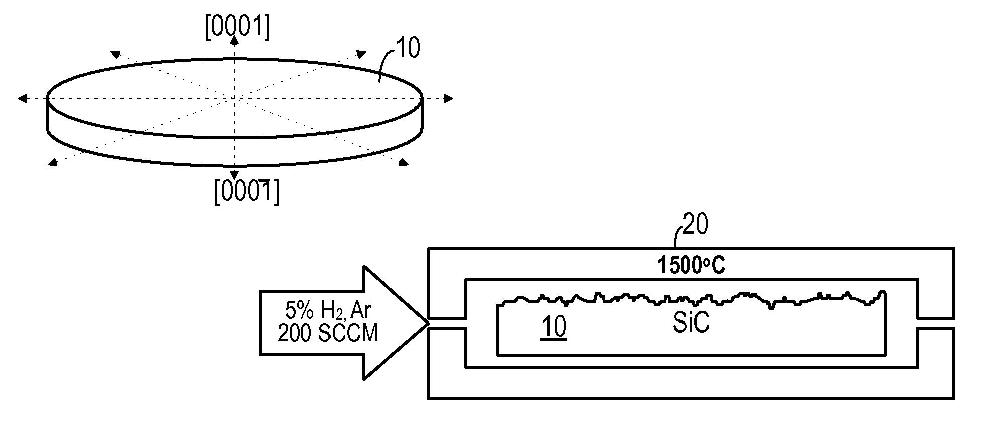
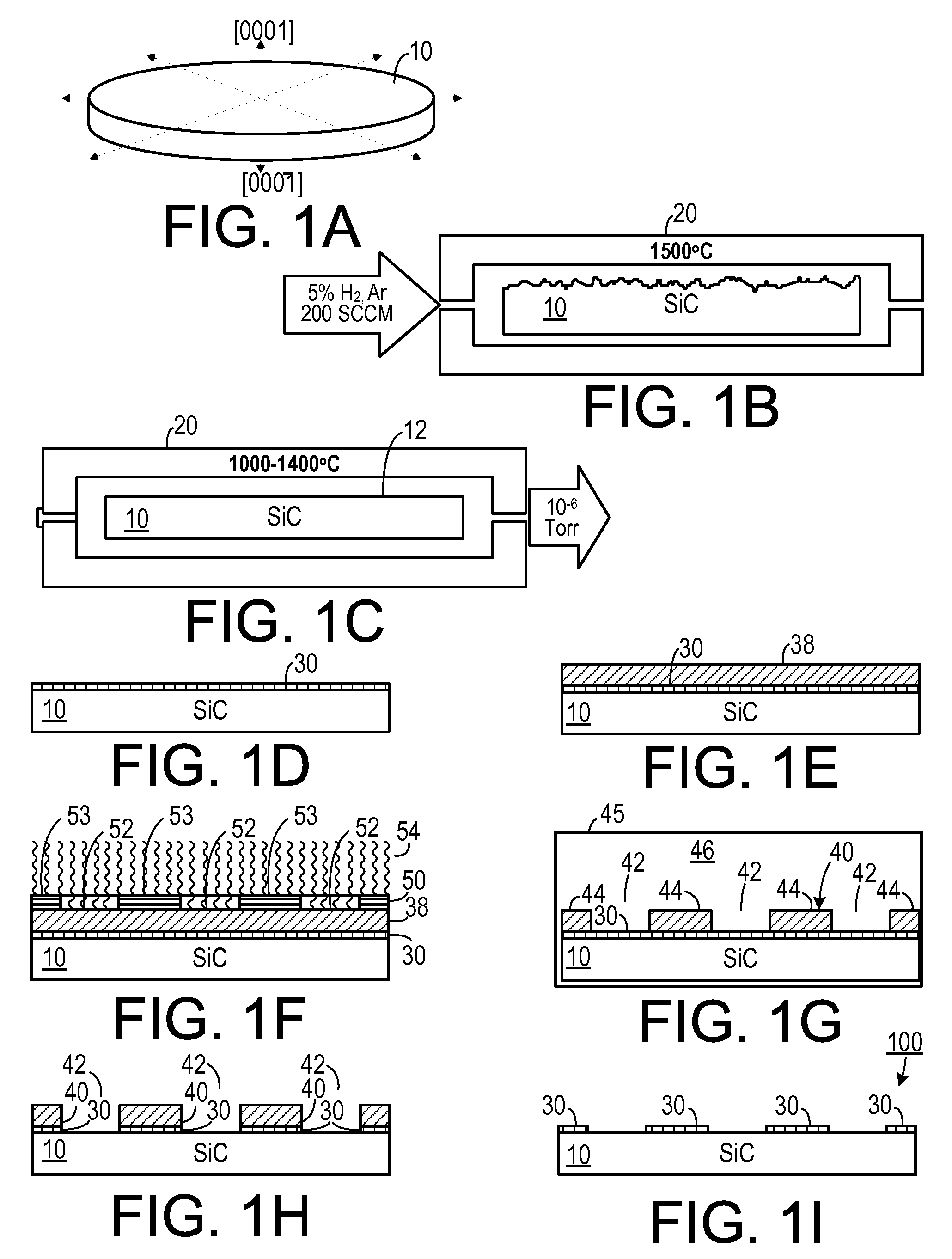
[0038]As shown in FIG. 1A, one method of making a device according to the invention begins with a substrate 10, such as a crystalline substrate. One example of a crystalline substrate includes silicon carbide. In one embodiment, a 6 H crystal of silicon carbide was used and a device according to the invention was produced on the [0001] face of the crystal. As will be appreci...


PUM

PropertyMeasurementUnit
currentsaaaaaaaaaa
sizesaaaaaaaaaa
pressureaaaaaaaaaa

Abstract

In a method of making graphite devices, a thin-film graphitic layer disposed against a preselected face of a substrate is created on the preselected face of the substrate. A preselected pattern is generated on the thin-film graphitic layer. At least one functionalizing molecule is attached to a portion of the graphitic layer. The molecule is capable of interacting with π bands in the graphitic layer.

Description

CROSS-REFERENCE TO A RELATED PATENT APPLICATION[0001]The present application claim is Continuation-in-Part of U.S. patent application Ser. No. 11 / 302,868, filed on Dec. 14, 2005 now U.S. Pat. No. 7,327,000, entitled “PATTERNED THIN FILM GRAPHITE DEVICES AND METHOD FOR MAKING SAME,” which is a Divisional application of U.S. patent application Ser. No. 10 / 860,710, filed on Jun. 03, 2004, entitled “PATTERNED THIN FILM GRAPHITE DEVICES AND METHOD FOR MAKING SAME,” which issued as U.S. Pat. No. 7,015,142 on Mar. 21, 2006, the entirety of which is incorporated herein by reference into the disclosure of the present application.CROSS-REFERENCE TO A PROVISIONAL PATENT APPLICATION[0002]The present application claims priority on U.S. Provisional Patent Application Ser. No. 60 / 798,651, filed on May 8, 2006, entitled “EXPANDING THE ELECTRONIC FUNCTIONALITY OF PATTERNED GRAPHITE STRUCTURES BY INCORPORATING MOLECULES IN NPEG STRUCTURES” and U.S. Provisional Patent Application Ser. No. 60 / 477,997, ...

Claims


Application Information

Patent Timeline
Patent Type & Authority Patents(United States)
IPC IPC(8): B32B9/00
CPCH01L21/0405H01L21/0445H01L21/8213H01L29/16H01L29/772H01L29/7781H01L29/1606Y10T428/30Y10S977/742Y10T428/31504
Inventor DEHEER, WALT A.
Owner GEORGIA TECH RES CORP
Why Eureka
Try Eureka