
Electronic components and methods for producing same

a technology applied in the field of electronic components and methods for producing same, can solve the problems of material deformation when pressed into the cut slot, low-cost electronics, and inapplicability to high-resolution lithographic procedures, and achieve the effect of producing electronic components and avoiding the lowest possible technological expens

Active Publication Date: 2011-09-06
CUFER ASSET LTD LLC
View PDF30 Cites 2 Cited by
  • Summary
  • Abstract
  • Description
  • Claims
  • Application Information

AI Technical Summary

Benefits of technology

[0010]It is therefore the task of the invention to develop one or more methods with which closely adjacent electrodes may be structured on a substrate in a simple, low-cost manner, and thus allow the production of electronic components with the least possible technological expense.

Problems solved by technology

However, these high-resolution lithographic procedures are very cost-intensive and therefore not suitable for the application realms of low-performance, low-cost electronics.
The disadvantage here, however, is that the material is deformed when pressed into the cut slot, and the opposing sidewalls of the channel are positioned very close to each other.
The active layer subsequently deposited cannot be evenly distributed because of meniscus formation.

Method used


Image

  • Electronic components and methods for producing same
  • Electronic components and methods for producing same
  • Electronic components and methods for producing same

Examples


Embodiment Construction

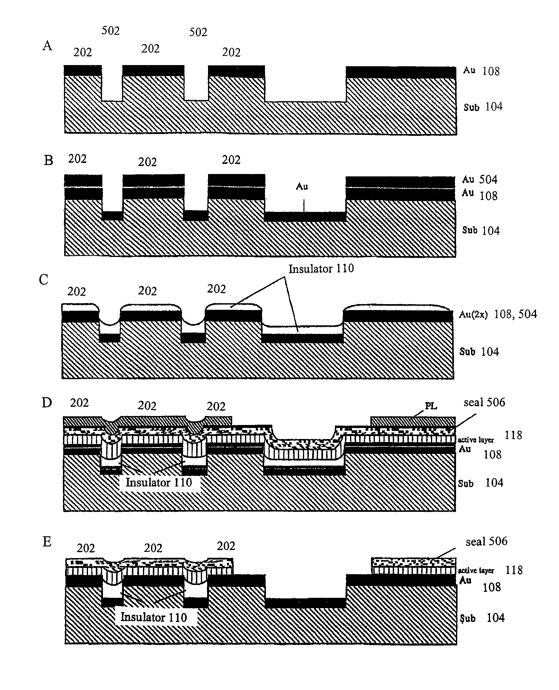
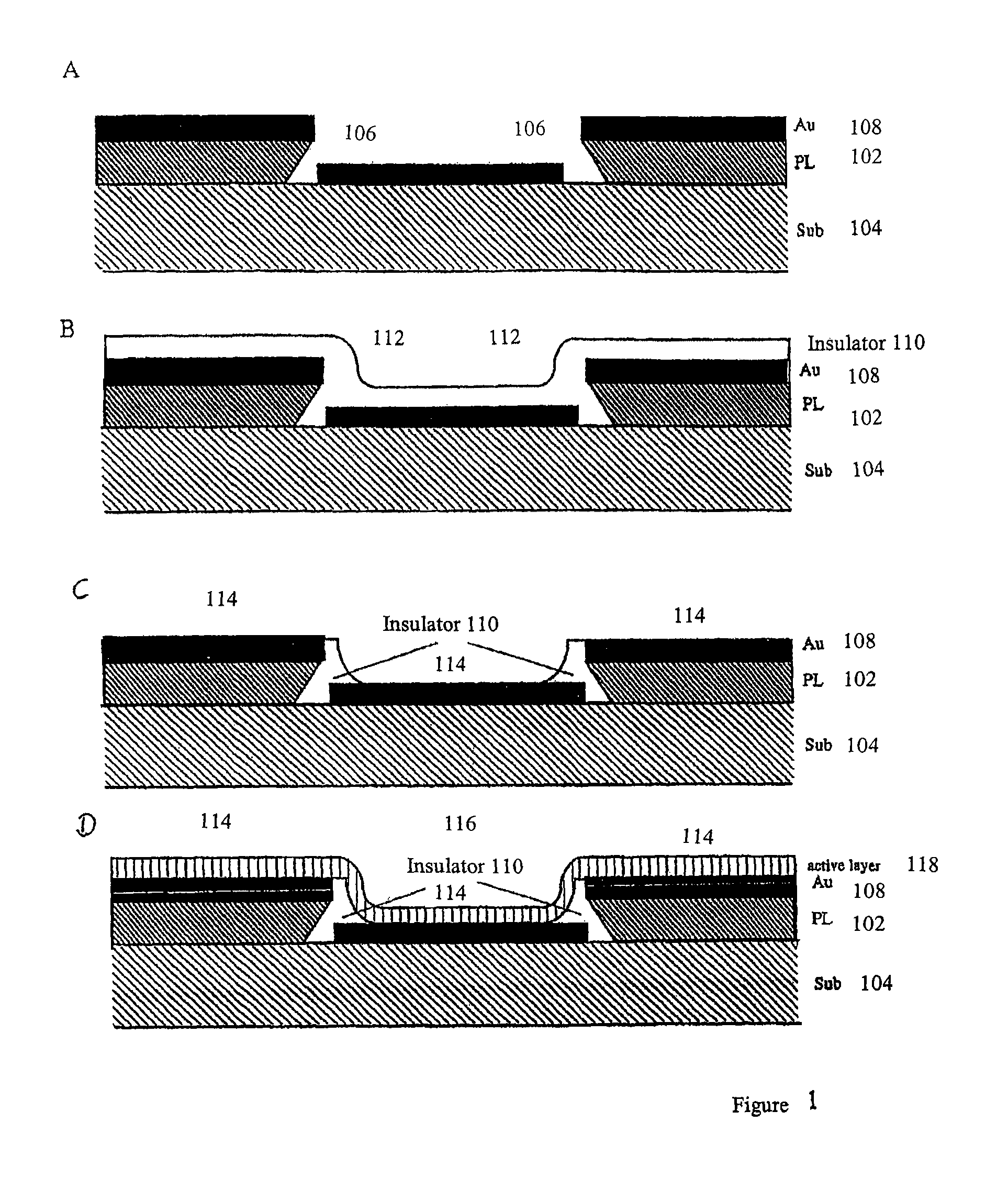
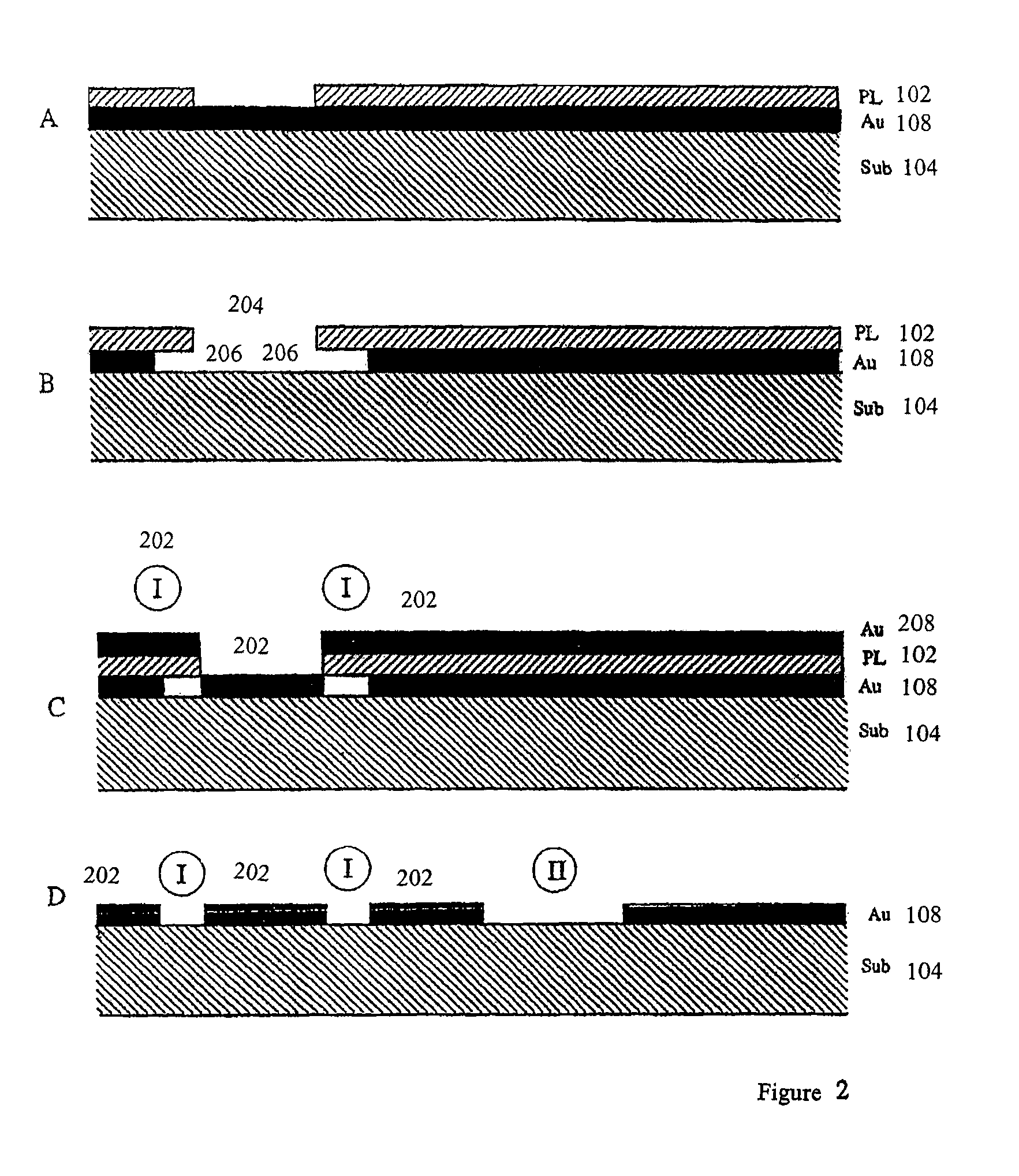
[0018]FIG. 1 shows the steps of a vertical production method. A photo lacquer 102 was deposited on a substrate 104 and was so structured that overlapping edges arise 106 on the photo lacquer 102. Subsequently, a metal vapor 108, preferably Chromium or Gold, is deposited. The insulator 110 applied in the subsequent procedure step covers the entire surface. Flat edges 112 are formed on the overlapping edges 106 of the photo lacquer 102 because of meniscus formation during the subsequent etching process as an inverse of the overlaps. The substrate 104 with its mounted and insulated electrodes 114 thus produced may be completed to produce a field-effect transistor 116 in subsequent procedure steps such as scattering the organic semiconductor (‘active layer’) 118, deposition of another insulator, and gate metallization and exposure of the electrodes 114.

[0019]FIG. 2 shows another method to structure closely adjacent electrodes 202 on a substrate 104. In this method, a metal vapor 108, pr...


PUM


Abstract

The invention relates to a method for producing electronic components comprising adjacent electrodes interspaced at distances ranging between 10 nanometers and several micrometers on a substrate of any type. According to the invention, the electrodes are structured by means of overlapping edges on the deposited layer or by undercutting the deposited layers. The electronic components are then produced either in the conventional manner or using a lithographic process from the underside of the transparent substrate and finally by means of a succession of known method steps for the production of electronic components.

Description

CROSS-REFERENCE TO RELATED APPLICATIONS[0001]This application is the National Stage of International Application No. PCT / EP04 / 09729, filed Sep. 1, 2004.BACKGROUND[0002]1. Field of the Invention[0003]The invention relates to several methods for producing electronic components with adjacent electrodes tightly interspaced at distances ranging between 10 nanometers and several micrometers on a substrate of any type that may also be a polymer film or glass, except for substrates for standard semiconductor technology such as Si, SiO2, Si3N4, GaAs, Al2O3.[0004]The methods based on the invention find application in the extremely low-cost and simple manufacture of electronic components requiring the smallest electrode separation such as, for example, molecular electronics, polymer field-effect transistors or field emitters.[0005]2. Description of Related Art[0006]The State of the Art describes various lithographic procedures (DUV or electron-beam lithography) by means of which the shortest p...

Claims


Application Information

Patent Timeline
Patent Type & Authority Patents(United States)
IPC IPC(8): H01L51/40H01L21/027
CPCH01L51/0023H01L51/0545H01L21/0272H10K71/621H10K10/466
Inventor DOLL, THEODORSCHEINERT, SUSANNESCHERER, AXELPAASCH, GERNOT
Owner CUFER ASSET LTD LLC
Learn More