Substrate of a liquid crystal display panel, liquid crystal panel and manufacturing method thereof

a liquid crystal display panel and substrate technology, applied in non-linear optics, instruments, optics, etc., can solve the problems of image displaying defect, poor image quality, and product quality disadvantages in some degr

Active Publication Date: 2011-09-27
BEIJING BOE OPTOELECTRONCIS TECH CO LTD +1
View PDF11 Cites 2 Cited by
  • Summary
  • Abstract
  • Description
  • Claims
  • Application Information

AI Technical Summary

Problems solved by technology

In the traditional manufacturing process of a TFT-LCD, since the bonding deflection within a certain range arises in the assembling process of the color filter substrate and the array substrate, the product quality is disadvantageously affected to some extent.
Where the deflection goes beyond the well-established standard, not only the black matrix cannot fun

Method used


Image

  • Substrate of a liquid crystal display panel, liquid crystal panel and manufacturing method thereof
  • Substrate of a liquid crystal display panel, liquid crystal panel and manufacturing method thereof
  • Substrate of a liquid crystal display panel, liquid crystal panel and manufacturing method thereof

Examples


fifth embodiment

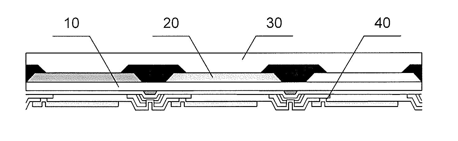
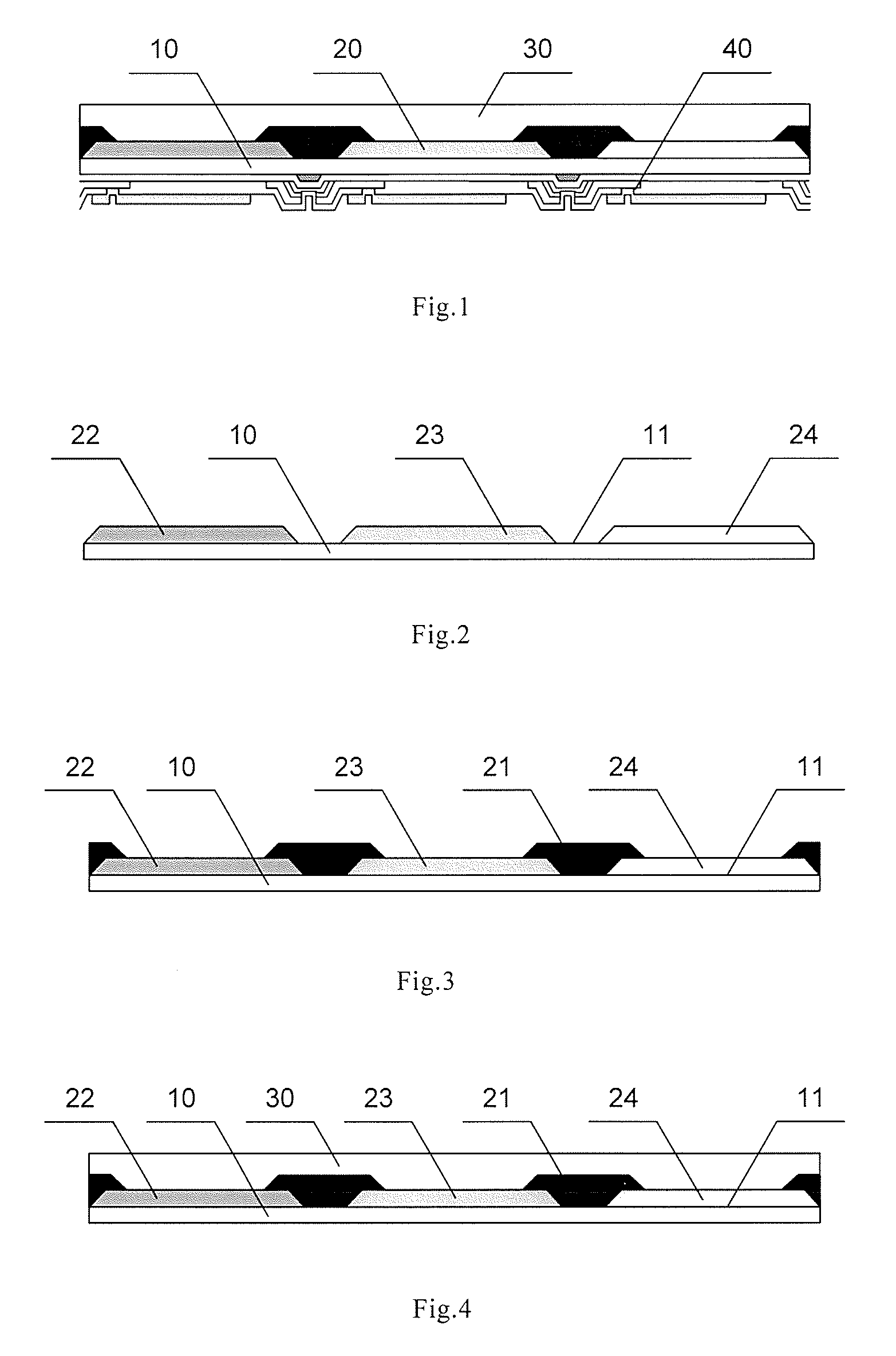
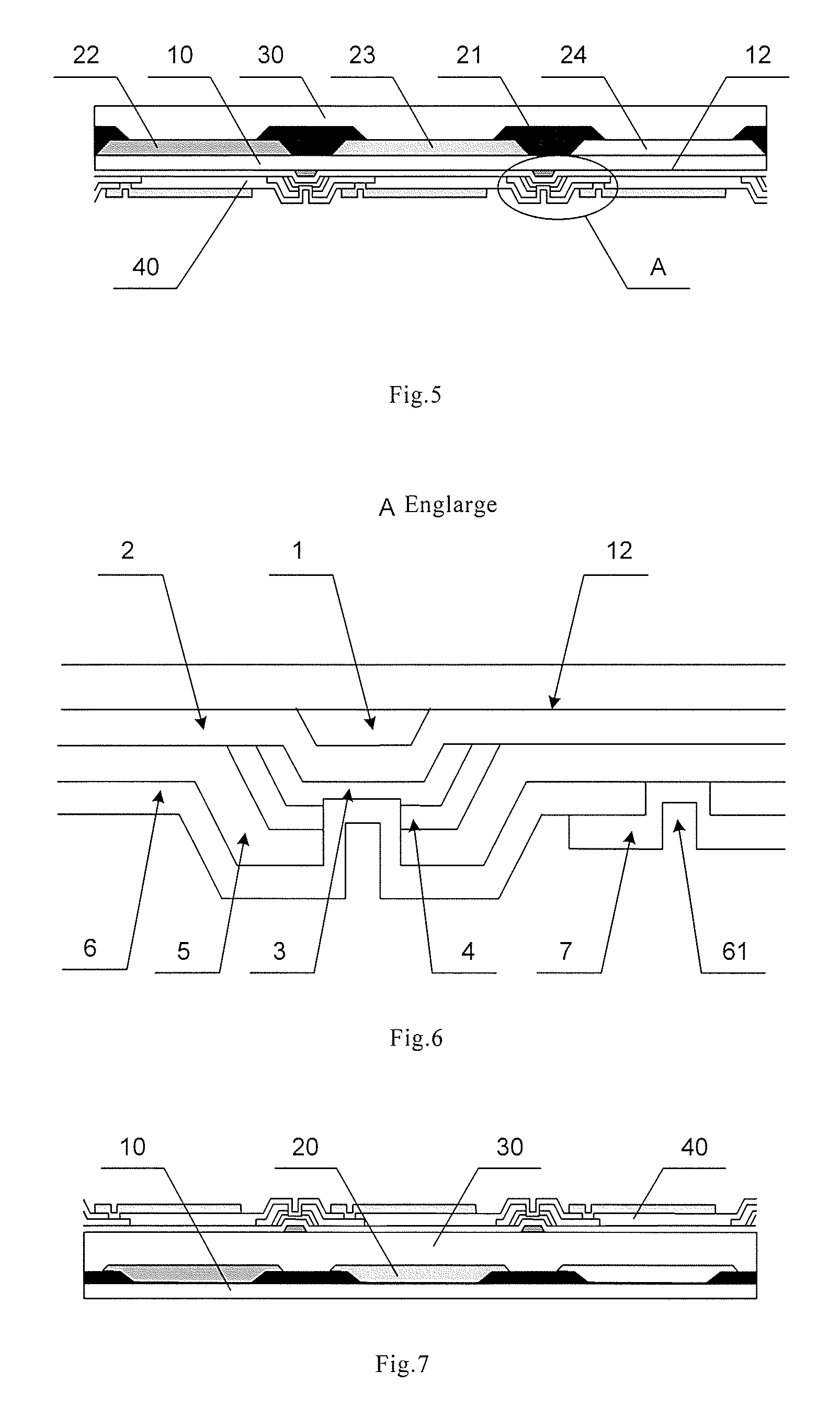
FIG. 15 is a flow chart of a manufacturing method of a substrate of a LCD panel according to the invention, and the manufacturing method may comprise:

step 11, forming a red color resin, a green color resin, and a blue color resin on one surface of a first substrate;

step 12, forming a black matrix on the first substrate after step 11;

step 13, forming a transparent layer with a planar surface on the same surface of the first substrate after step 12; and

step 14, forming an array structure layer on the other surface of the first substrate after step 13.

In addition, step 11 and step 12 may further comprise the step of forming an alignment mark, and the alignment mark is used as the alignment reference for forming the array structure layer subsequently, so that the color filter layer and the array structure layer can be aligned accurately with an alignment deflection of less than about 1.5 μm.

In step 11, the red color resin, the green color resin, and the blue color resin are sequentially...


PUM


Abstract

Embodiments of the present invention provide a substrate of a liquid crystal display (LCD) panel, a liquid crystal panel, and a manufacturing method thereof. The substrate of a LCD panel comprises a first substrate, a color filter layer comprising color resins and a black matrix and formed on one surface of the first substrate, a transparent layer formed on the color filter layer and having a planar surface, and an array structure layer formed on the planar surface of the transparent layer or on the other surface of the first substrate.

Description

BACKGROUNDThe present invention relates to a thin film transistor liquid crystal display and a manufacturing method thereof.Thin film transistor liquid crystal displays (TFT-LCDs) have the advantages of small volume, low power consumption, no radiation and so on and is becoming dominant in the current planar panel display market.A traditional TFT-LCD comprises an array substrate, a color filter substrate, and liquid crystal material filled between the two substrates. The displaying mechanism of a TFT-LCD is that the electric field formed between the color filter substrate and the array substrate renders the liquid crystal molecules orientated, and the twisting angle of the liquid crystal molecules can be controlled by the electric field, intensity of which is adjusted by varying the applied voltage, so that the amount of light transmitted through pixels can be controlled and the desired image can be obtained. The array substrate comprises gate lines, data lines, pixel electrodes, an...

Claims


Application Information

Patent Timeline
IPC IPC(8): G02F1/1335
CPCG02F1/133512G02F1/133514G02F2001/133354G02F2001/136222G02F1/136209G02F2001/133562G02F1/133354G02F1/133562G02F1/136222
Inventor SHI, YUE
Owner BEIJING BOE OPTOELECTRONCIS TECH CO LTD
Why Eureka
Try Eureka