Semiconductor device, light emitting diode head, and image forming apparatus

a technology of light-emitting diodes and semiconductor devices, which is applied in the direction of semiconductor/solid-state device details, instruments, electrographic processes, etc., can solve the problems of lowering energy efficiency and increasing the potential difference between connecting portions, so as to reduce the length of the wiring pattern of the electrode connection structure, improve the energy efficiency of the image forming apparatus, and minimize the effect of voltage drop

Inactive Publication Date: 2011-10-11
OKI DATA CORP
View PDF5 Cites 4 Cited by
  • Summary
  • Abstract
  • Description
  • Claims
  • Application Information

AI Technical Summary

Benefits of technology

[0018]In the present invention, the first conductive type semiconductor layer and the second conductive type semiconductor layer are disposed on the substrate, so that it is possible to shear a common electrode connection structure of the second conductive type semiconductor layer. Accordingly, it is possible to reduce a wiring pattern length of an electrode connection structure of the first conductive type semiconductor layer as well. As a result, it is possible to minimize voltage drop due to wiring resistance, thereby improving energy efficiency of the image forming apparatus as a whole.
[0019]In the semiconductor device of the present invention, when the light emitting elements are a selective diffusion type for emitting light in a range from red to infra read, it is preferred to diffuse a p-type impurity into an n-type semiconductor layer, as opposed to diffusing an n-type impurity into a p-type semiconductor layer, due to a lower annealing temperature in a diffusion process. Accordingly, it is possible to easily produce a diffused area with a lower resistivity, and to produce an LED array with improved element characteristics.

Problems solved by technology

Further, the wiring pattern is connected to an electrode pad to be connected to a drive element over a relatively long distance, thereby increasing a potential difference between connecting portions and lowering energy efficiency.

Method used


Image

  • Semiconductor device, light emitting diode head, and image forming apparatus
  • Semiconductor device, light emitting diode head, and image forming apparatus
  • Semiconductor device, light emitting diode head, and image forming apparatus

Examples


first embodiment

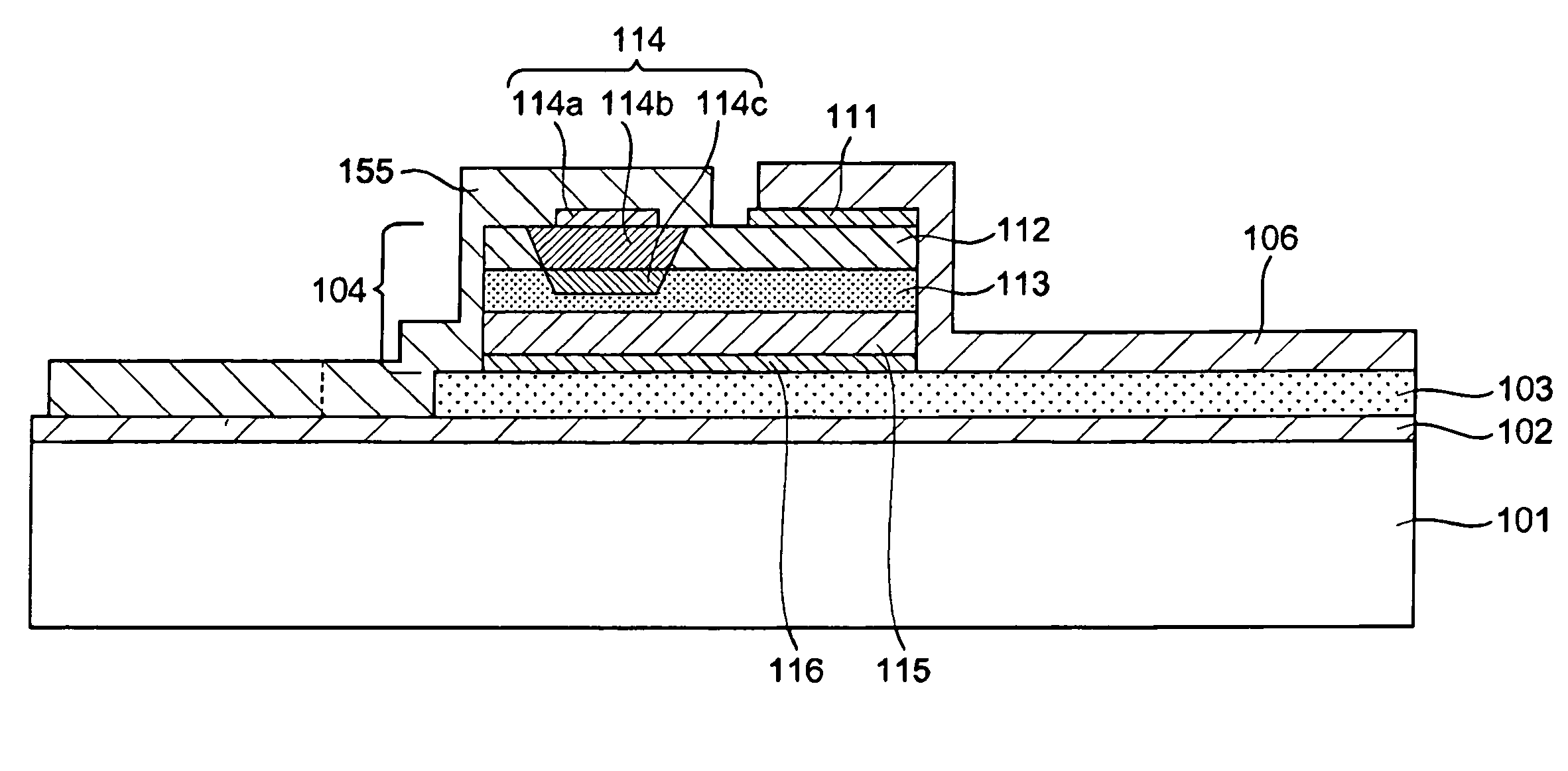
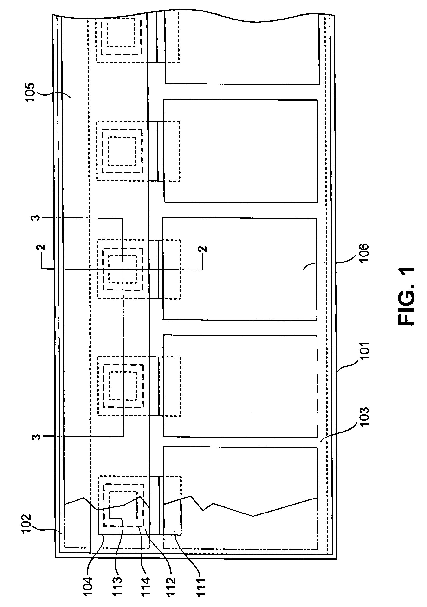
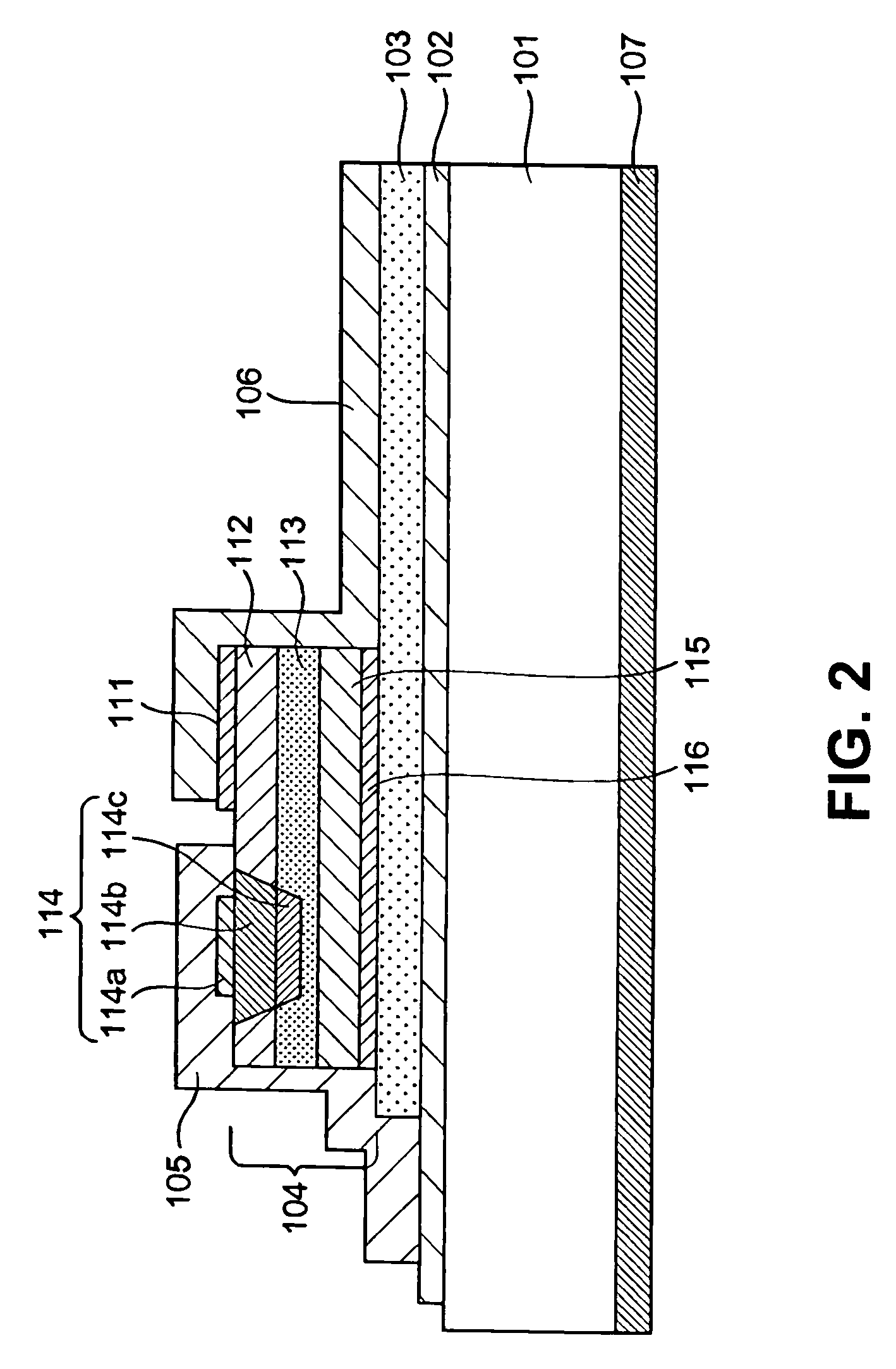
[0052]A first embodiment of the present invention will be explained. FIG. 1 is a schematic plan view showing a semiconductor device according to the first embodiment of the present invention. FIG. 2 is a schematic sectional view of the semiconductor device taken along a line 2-2 in FIG. 1 according to the first embodiment of the present invention. FIG. 3 is a schematic sectional view of the semiconductor device taken along a line 3-3 in FIG. 1 according to the first embodiment of the present invention. The semiconductor device is an example of a light emitting diode (LED) array driven through a concurrent drive. The semiconductor device is especially preferred to provide an LED head of an image forming apparatus such as a photoelectric printer.

[0053]As shown in FIG. 1 to FIG. 3, a conductive layer 102 made of a metal layer and an insulation layer 103 made of an organic thin layer are laminated on a main surface of a p-type silicon substrate 101. The p-type silicon substrate 101 is e...

second embodiment

[0067]A second embodiment of the present invention will be explained next. FIG. 4 is a schematic plan view showing a semiconductor device according to the second embodiment of the present invention. FIG. 5 is a schematic sectional view of the semiconductor device taken along a line 5-5 in FIG. 4 according to the second embodiment of the present invention. FIG. 6 is a schematic plan view showing the semiconductor devices arranged in a group according to the second embodiment of the present invention.

[0068]As shown in FIGS. 4 and 5, the p-side electrode contact layer 155 is formed partially to expose the conductive layer 102 as a conductive layer exposure area 121 on the main surface of the substrate, so that the common potential is supplied from an upper surface. When the conductive layer exposure area 121 is used to connect externally through a wire bonding or the like, the conductive layer 102 may have a thickness between 500 nm and 1 μm in the conductive layer exposure area 121. T...

third embodiment

[0070]A third embodiment of the present invention will be explained next. FIG. 7 is a schematic plan view showing a semiconductor device according to a third embodiment of the present invention. FIG. 8 is a schematic sectional view of the semiconductor device taken along a line 8-8 in FIG. 7 according to the third embodiment of the present invention.

[0071]In the third embodiment, the LED array is a split drive type, while the LED array in the first embodiment is the concurrent drive type.

[0072]As shown in FIG. 7, the LED array is divided into two LED blocks. A p-type area of each block is supplied with the common potential, and an n-type area of each LED is supplied with a separate potential through switching. A p-side wiring pattern 722 for supplying the common potential and an n-side wiring pattern 723 for supplying a separate potential are provided on a substrate 201. The p-side wiring pattern 722 is connected to a p-side electrode pad 726, and the n-side wiring pattern 723 is co...


PUM


Abstract

A semiconductor device includes a substrate; a first conductive type semiconductor layer disposed on a main surface of the substrate; a second conductive type semiconductor layer disposed on the first conductive type semiconductor layer; a plurality of light emitting elements; and a second conductive side wiring pattern for commonly connecting the second conductive type semiconductor layer in the light emitting elements arranged adjacently. The second conductive type semiconductor layer includes a first conductive type semiconductor connection surface and a second conductive type semiconductor connection surface between the first conductive type semiconductor layer.

Description

BACKGROUND OF THE INVENTION AND RELATED ART STATEMENT[0001]The present invention relates to a semiconductor device of a light emitting diode (LED) array and the likes, in which a plurality of light emitting elements is arranged; a light emitting diode (LED) head including the semiconductor device; and an image forming apparatus including the light emitting diode (LED) head.[0002]In a conventional image forming apparatus such as a printer using electro-photography technology, a plurality of light emitting diodes (LEDs) is arranged to form an LED array chip, and a plurality of the LED array chips is arranged to form a light emitting diode (LED) head. Recently, it has been required that an image forming apparatus such as a printer forms an image with high resolution. Accordingly, the number of the light emitting elements in the LED print head has increased drastically.[0003]In the LED array chip, an impurity is diffused in a surface of a semiconductor compound wafer (such as GaAs) thro...

Claims


Application Information

Patent Timeline
Patent Type & Authority Patents(United States)
IPC IPC(8): H01L29/18H01L33/08H01L33/30H01L33/34H01L33/38H01L33/40
CPCB41J2/45G03G15/326G03G15/04054H01L27/153G03G2215/0409
Inventor OGIHARA, MITSUHIKOFUJIWARA, HIROYUKIMUTO, MASATAKASUZUKI, TAKAHITOIGARI, TOMOKI
Owner OKI DATA CORP
Why Eureka
Try Eureka