Flash file system

a file system and flash memory technology, applied in the field of electronic storage, can solve the problems of inefficient write operation, limited life of flash memory, and high manufacturing cost, and achieve the effect of being adaptable to specific applications

Active Publication Date: 2011-10-18
SAMSUNG ELECTRONICS CO LTD
View PDF5 Cites 32 Cited by
  • Summary
  • Abstract
  • Description
  • Claims
  • Application Information

AI Technical Summary

Benefits of technology

[0008]The flash file system according to the present invention has a hierarchical structure that permits redesigning a host system, flash memory or a portion of the flash file system without completely redesigning the flash file system. Accordingly, the flash file system of the present invention is extremely flexible and readily adaptable to specific applications.

Problems solved by technology

The NOR type of flash memory provides for random access, but is expensive to manufacture.
The NAND type of flash memory, on the other hand, is relatively inexpensive but suffers from an inefficient write operation.
Besides being inefficient, this erase before write, or EBW, process means the flash memory has a limited lifetime.
Because of this, such types of memory have a finite number of erase-write cycles because the dielectric eventually deteriorates.
Storing this information in the flash memory itself reduces the storage capacity of the flash memory, and can also result in configurations of the flash memory which are difficult to manage.

Method used


Image

  • Flash file system
  • Flash file system
  • Flash file system

Examples


Embodiment Construction

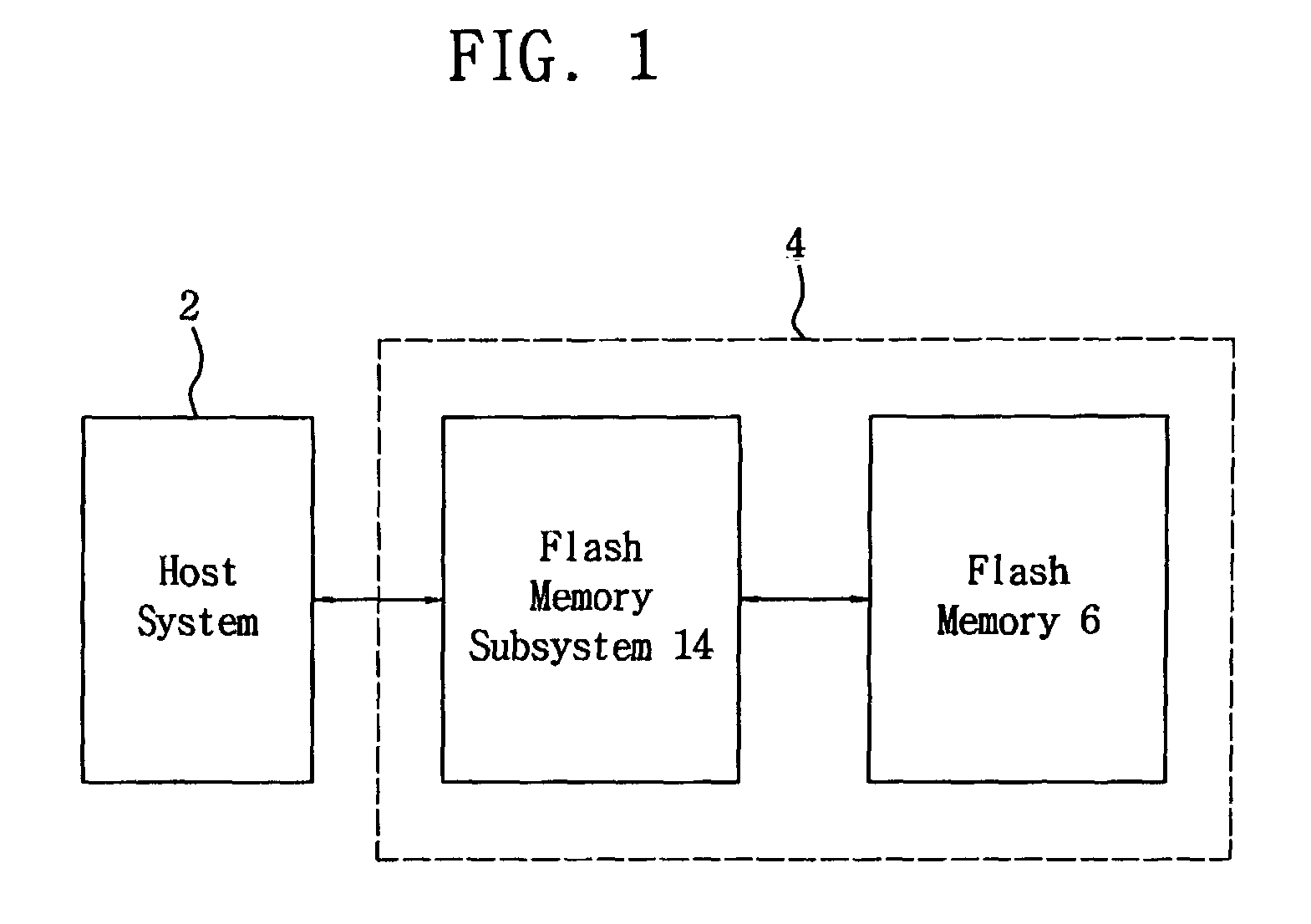
[0027]FIG. 1 illustrates a host system 2 connected to a flash file system 4 according to an exemplary embodiment of the present invention. As shown, the flash file system includes a flash memory 6 connected to a flash memory subsystem 14. The flash memory 6 is a NAND type flash memory. The flash memory subsystem 14 serves as an interface between the host system 2 and the flash memory 6.

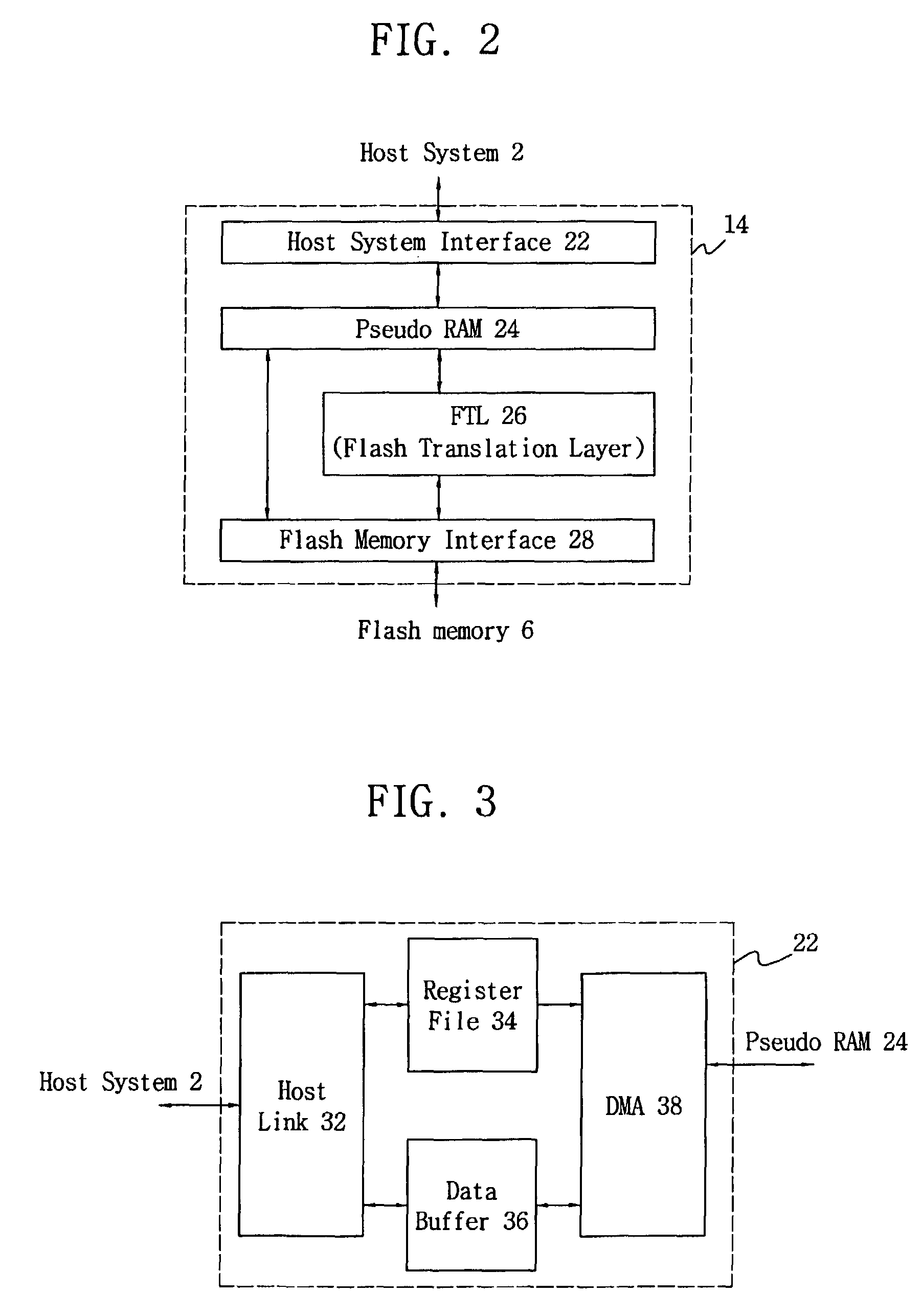
[0028]FIG. 2 illustrates the flash memory subsystem 14 in greater detail. As shown, the flash memory subsystem 14 has a hierarchical structure. As a result, redesign of the flash memory 6 or host system 2 does not require an entire redesign of the flash memory subsystem 14. Namely, as shown, the flash memory subsystem 14 includes a host system interface 22 that interfaces with the host system 2. A pseudo RAM 24 connected to the host system interface 22 operates as a form of cache, and temporarily stores data being written into and read from the flash memory 6. A flash translation layer unit (FTL) 26 m...


PUM


Abstract

The flash file system includes a flash memory and a subsystem interfacing between the flash memory and a host system. The subsystem includes a hierarchical structure of a host system interface, cache memory system, flash translation layer unit and a flash memory interface. The host system interface interfaces with the host system. The cache memory system has a storage capacity of a predetermined number of data units and stores data for transfer to and from the host system via the host system interface. The flash translation layer unit maps a logical address received from the host system via the host system interface and the cache memory into a physical address of the flash memory. The flash memory interface interfaces with the flash memory to transfer data to the flash memory from the cache memory system based on the physical address received from the flash translation layer unit and to transfer data from the flash memory to the cache memory system based on the physical address received from the flash translation layer unit.

Description

BACKGROUND OF THE INVENTION[0001]The present invention relates to the field of electronic storage. More particularly, the invention is directed towards flash memory and a file system therefore. Flash memory is becoming more and more widely used because information stored in a flash memory is maintained even when power is no longer supplied to the flash memory. Furthermore, flash memory is a solid state device and is extremely useful for portable devices such as portable computers, digital still cameras, etc. A flash memory consumes much less power and is not susceptible to shocks as are many types of magnetic storage media such as hard disks.[0002]There are two types of flash memory, a NAND type and a NOR type. The NOR type of flash memory provides for random access, but is expensive to manufacture. The NAND type of flash memory, on the other hand, is relatively inexpensive but suffers from an inefficient write operation.[0003]When a portion of the flash memory has previously been p...

Claims


Application Information

Patent Timeline
Patent Type & Authority Patents(United States)
IPC IPC(8): G06F12/00G06F12/10G06F3/06G06F12/02G06F12/08
CPCG06F3/0616G06F3/0643G06F3/0679G06F12/0292G06F12/0866G06F12/0246G06F2212/7201G06F2212/222G06F12/08
Inventor LEE, JINAEON
Owner SAMSUNG ELECTRONICS CO LTD
Why Eureka
Try Eureka