

Noncontact IC label and method and apparatus for manufacturing the same
a technology of non-contact ic labels and manufacturing methods, applied in the direction of semiconductor/solid-state device details, near-field systems using receivers, instruments, etc., to achieve the effects of high quality, high manufacturing efficiency, and sufficient electromotive for
- Summary
- Abstract
- Description
- Claims
- Application Information
AI Technical Summary
Benefits of technology
Problems solved by technology
Method used
Image

Examples
first embodiment
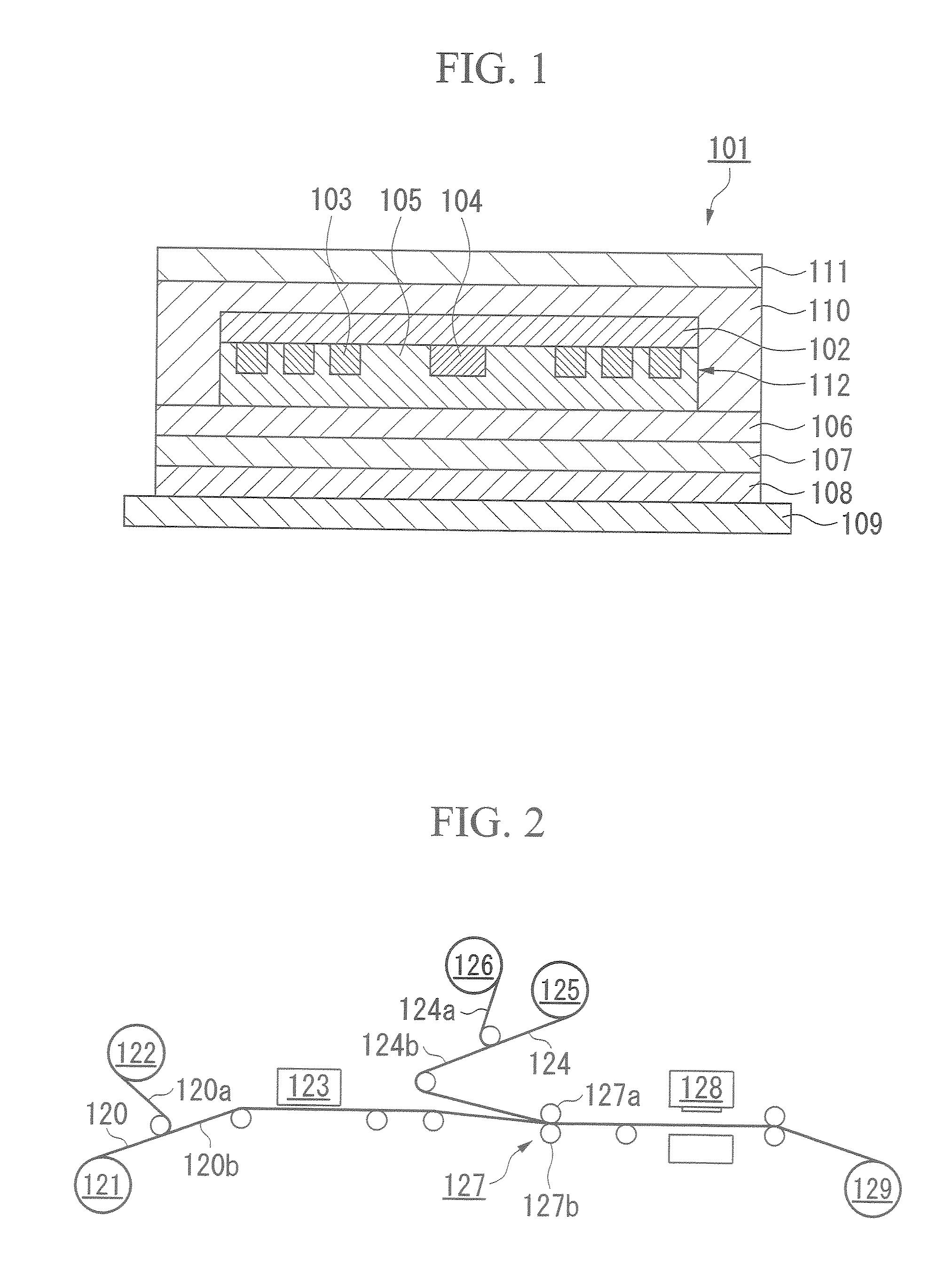
[0227]FIG. 1 is an outline sectional view of the non-contact IC label that is the present invention. In FIG. 1, an antenna coil 103 and an IC chip 104 are provided on one surface of an electrically insulating first substrate 102, with the antenna coil 103 and the IC chip 104 being electrically connected. On one surface of the first substrate 102, a magnetic layer 105 is provided so as to cover the antenna coil 103 and the IC chip 104, a first adhesive layer 106 is provided on the magnetic layer 105, an electrically insulating second substrate 107 is provided on the first adhesive layer 106, a second adhesive layer 108 is provided on the second substrate 107, and a release paper 109 is provided on the second adhesive layer 108. An overlay material 111 is provided on the other surface of the first substrate 102 via a third adhesive layer 110.
[0228]The first substrate 102 in this embodiment may be a publicly known material such as a woven fabric, non-woven fabric, mat, paper or combina...
second embodiment
[0242]FIG. 2 is a drawing schematically showing the constitution of the apparatus for manufacturing the non-contact IC label 101 according to the present invention.
[0243]The manufacturing apparatus of the present embodiment is provided with a first supply means 121 that supplies a first continuous sheet 120 consisting of a backing paper attached to one surface of the second substrate 107 via the first adhesive layer 106 and the release paper attached to the other surface via the second adhesive layer 108.
[0244]After a backing paper 120a on the surface layer of the first continuous sheet 120 supplied from the first supply means 121 is peeled off and taken up by a take-up portion 122, the first continuous sheet 120 is sent to an inlet attaching means 123.
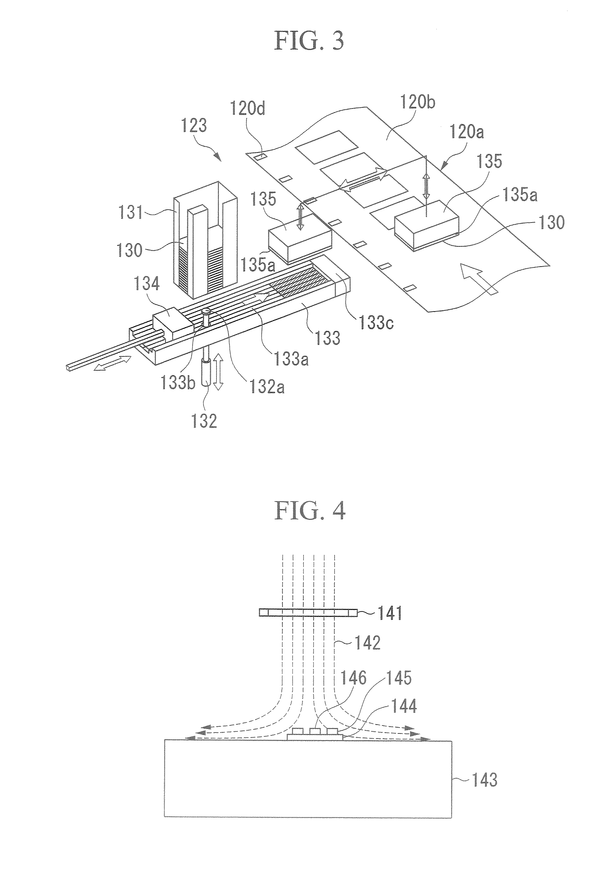
[0245]As shown in FIG. 3, the inlet attaching means 123 is provided with a stacker (holding means) 131 that holds a plurality of IC inlets 130 (corresponding to 112 in FIG. 1) in a vertically stacked state. Under the stacker 131, an i...
third embodiment
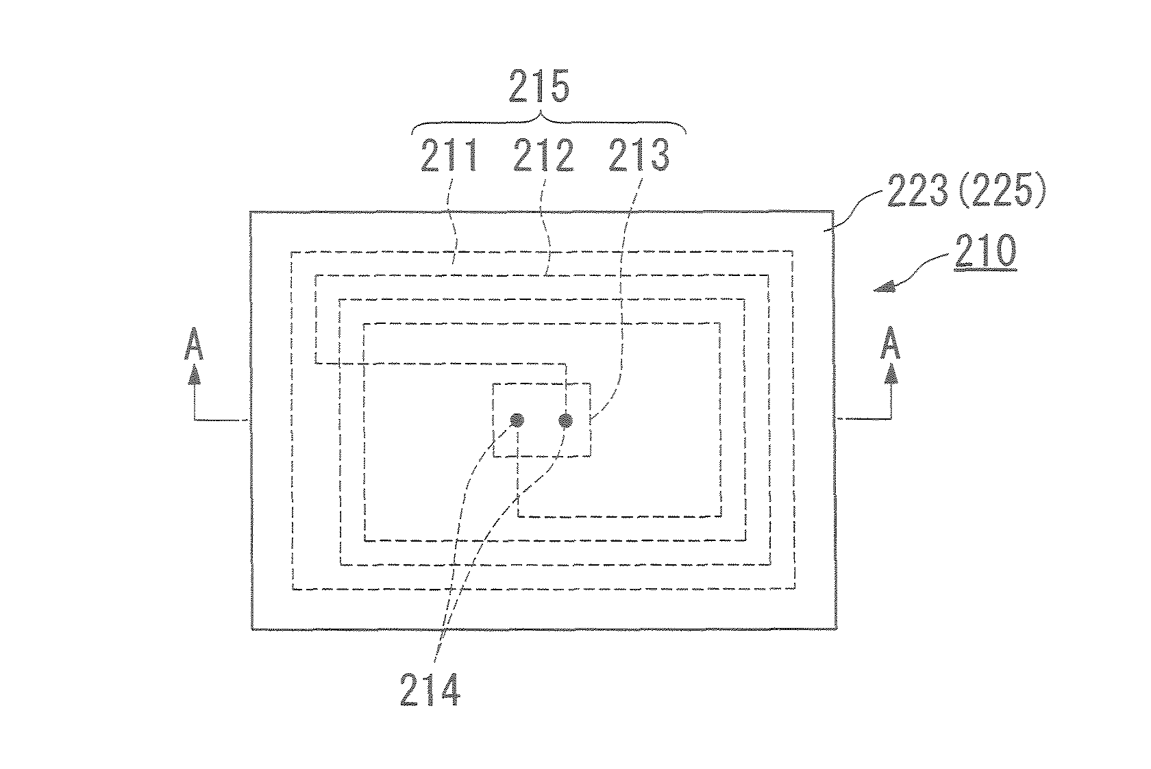
[0264]FIGS. 7A and 7B are schematic diagrams showing the non-contact IC tag that is the third embodiment according to the present invention, with FIG. 7A being a plan view showing the internal structure and FIG. 7B being a sectional view along line A-A of FIG. 7A.
[0265]In FIGS. 7A and 7B, reference numeral 210 denotes a non-contact IC tag, 211 a base substrate, 212 an antenna, 213 an IC chip, 214 contacts 215 an inlet, 220 a magnetic layer, 221 a first resin member 222 a recessed portion, 223 a second resin member, and 225 a case.
[0266]This non-contact IC tag 210 is roughly constituted from an inlet 215 including a base substrate 211 and an electrically connected antenna 212 and IC chip 213 provided on one surface thereof; a magnetic layer 220 disposed so as to cover the antenna 212 and the IC chip 213 constituting the inlet 215; and a case 225 including a first resin member 221 and a second resin member 223 provided so as to envelop the inlet 215 with the disposed magnetic layer 22...
PUM
 Abstract
Description
Claims
Application Information