Solid-state image pickup device, method of manufacturing solid-state image pickup device, and image pickup device

a solid-state image and pickup device technology, applied in the direction of color television, television system, radio control device, etc., can solve the problems of insufficient reduction of incident light blockage (shading), provision of large-angle ccd, high-speed ccd or the like, etc., to reduce the blockage of incident light, improve the sensitivity of light receiving unit, and reduce the effect of sensitivity

Inactive Publication Date: 2011-11-08
SONY CORP
View PDF1 Cites 0 Cited by
  • Summary
  • Abstract
  • Description
  • Claims
  • Application Information

AI Technical Summary

Benefits of technology

[0014]This solid-state image pickup device is for example of a 1 / 2.5-inch type with 2-μm pixel unit cells. The first transfer electrodes 111, the first wiring 121, and the second transfer electrodes 112 are generally made of polysilicon. The wiring width of the first wiring 121 and the second transfer electrodes 112 (second wiring) is about 300 nm. The film thickness of each of the first transfer electrodes 111, the first wiring 121, and the second transfer electrodes 112 is about 200 nm, from a viewpoint of reducing shading of light. The height of the first wiring 121 from the gate oxide film 103 is about 450 nm, for example, as shown in FIG. 21B. The light receiving unit 101 is surrounded on four sides (in the horizontal direction and the vertical direction) by walls about 450 nm high of the first transfer electrodes 111, the first wiring 121, and the second transfer electrodes 112. The walls surrounding the light receiving unit 101 on the four sides blocks incident light obliquely entering the light receiving unit 101, thus decreasing the sensitivity of the light receiving unit 101.
[0137]In addition, according to the solid-state image pickup device according to the above-described embodiment of the present invention, the first wiring and the second wiring serve also as a light shielding film, so that processes are reduced.

Problems solved by technology

However, the blockage (shading) of incident light cannot be reduced sufficiently with only the known single-layer transfer electrode structure, so that provisions cannot be made for a large-angle-of-view CCD, a high-speed CCD or the like.

Method used


Image

  • Solid-state image pickup device, method of manufacturing solid-state image pickup device, and image pickup device
  • Solid-state image pickup device, method of manufacturing solid-state image pickup device, and image pickup device
  • Solid-state image pickup device, method of manufacturing solid-state image pickup device, and image pickup device

Examples


first embodiment

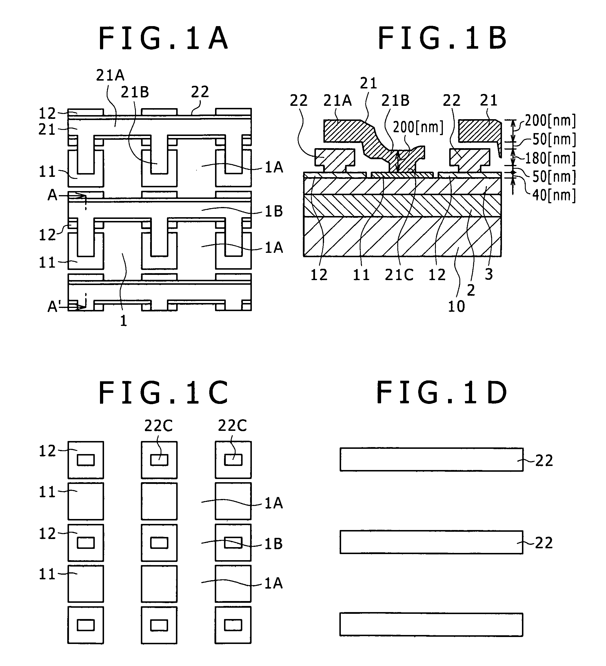
[0165]FIGS. 1A, 1B, 1C, and 1D are diagrams showing a solid-state image pickup device according to a first embodiment. FIG. 1A is a plan view, FIG. 1B is a sectional view taken along the line A-A′ of FIG. 1A, FIG. 1C is a diagram of assistance in explaining a part of transfer electrodes in FIG. 1A, and FIG. 1D is a diagram of assistance in explaining a part of second wiring in FIG. 1A.

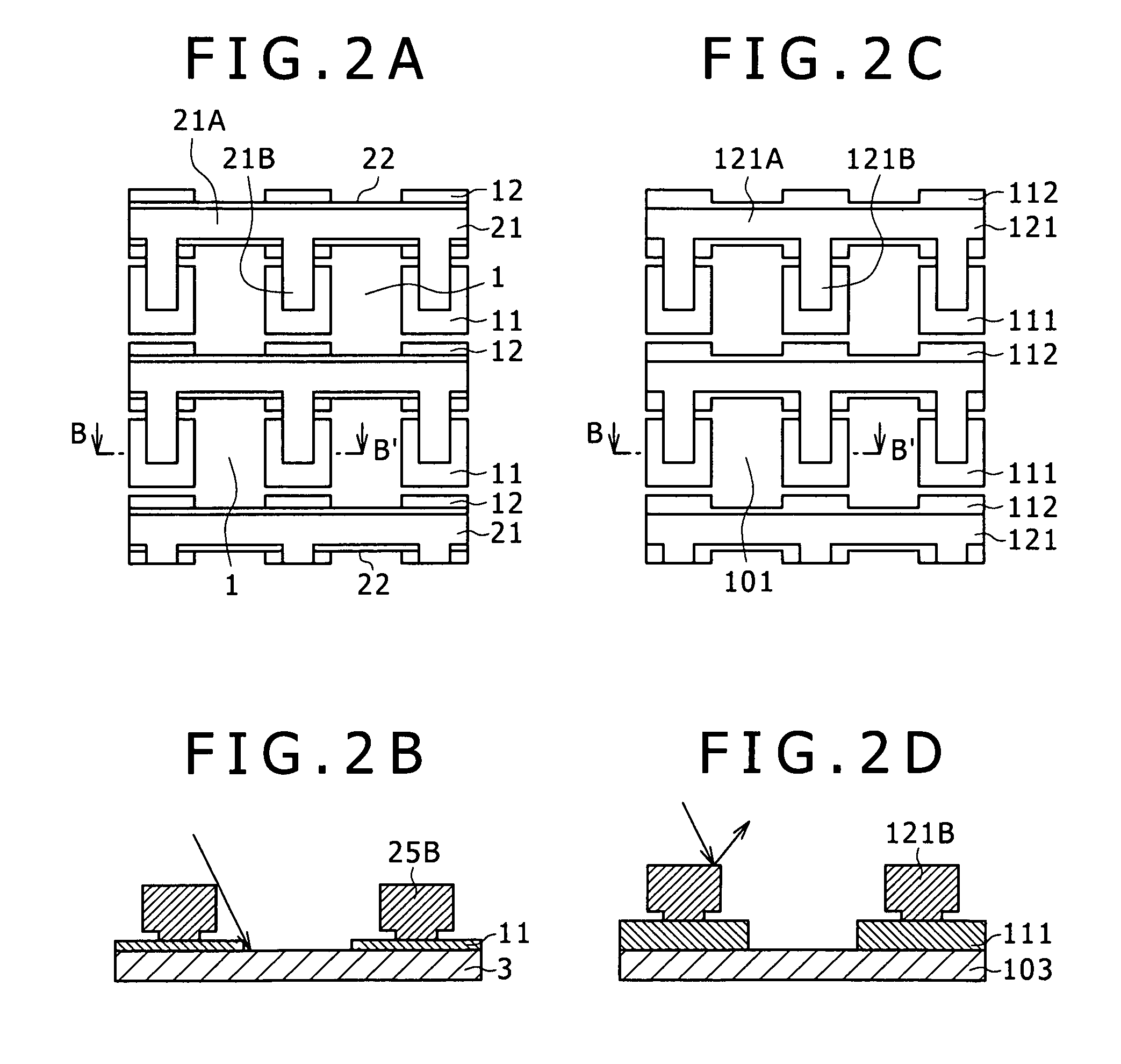
[0166]FIG. 2A is a plan view of the solid-state image pickup device according to the first embodiment which device is shown in FIGS. 1A, 1B, 1C, and 1D. FIG. 2B is a sectional view taken along the line B-B′ of FIG. 2A. FIG. 2C is a plan view of the solid-state image pickup device in the past shown in FIGS. 26A, 26B, and 26C. FIG. 2D is a sectional view taken along the line B-B′ of FIG. 2C.

[0167]The solid-state image pickup device is an example of a four-phase driving CCD. As shown in FIG. 1A and FIG. 2A, the solid-state image pickup device has a plurality of light receiving units 1 arranged in the form...

second embodiment

[0192]FIGS. 12A and 12B are diagrams showing a solid-state image pickup device according to a second embodiment. FIG. 12A is a plan view, and FIG. 12B is a sectional view taken along the line A-A′ of FIG. 12A.

[0193]As shown in FIGS. 12A and 12B, the solid-state image pickup device according to the second embodiment is formed by replacing the first wiring 21 in the solid-state image pickup device according to the first embodiment which device is shown in FIGS. 1A to 1D and FIGS. 2A and 2B with first wiring 23 made of a metal. Other parts form a similar constitution to that of the solid-state image pickup device according to the first embodiment, and are identified by the same reference numerals. Description of the other parts will be omitted.

[0194]The metal of the first wiring 23 is desirably W, Al, or Ti, for example. However, the metal of the first wiring 23 may be Cu, Ta, Pt, Ir, or Ru. In addition, the metal of the first wiring 23 may be an alloy of at least two of Al, Ti, Cu, Ta...

third embodiment

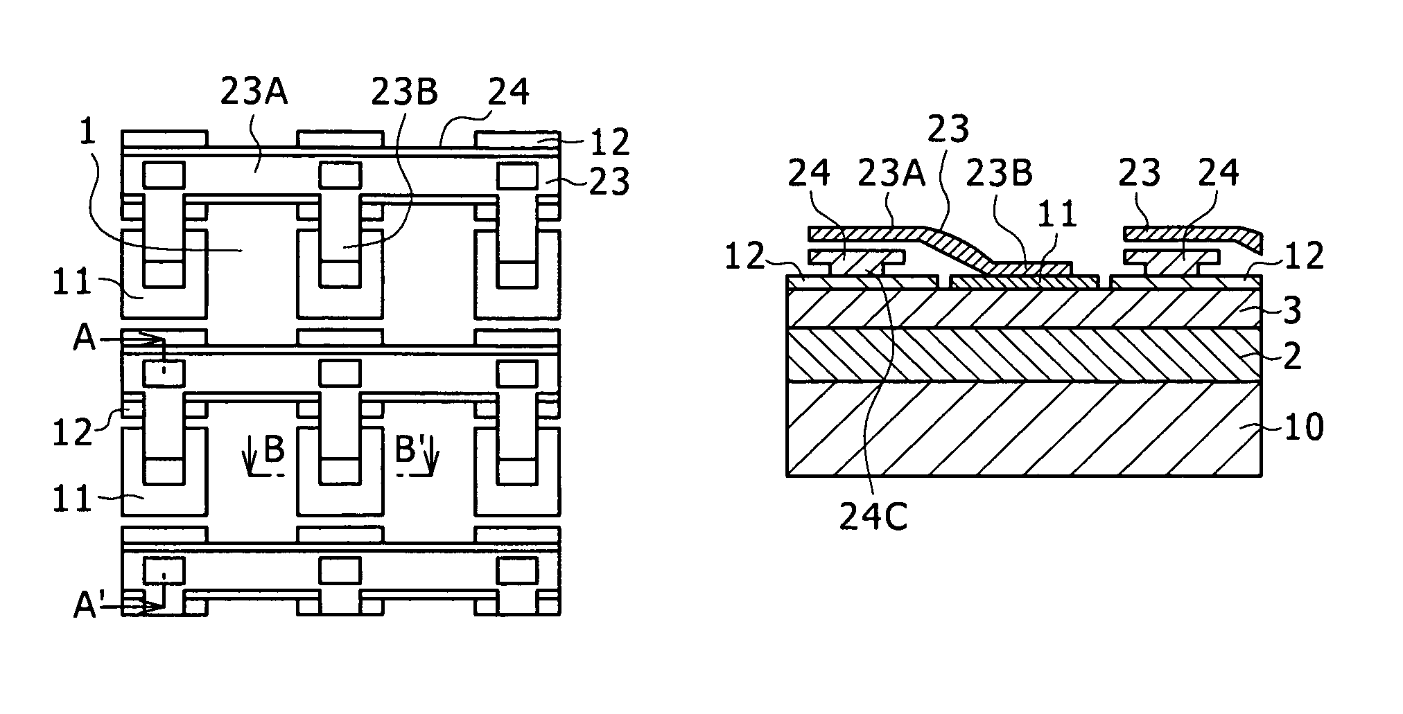
[0198]FIGS. 13A, 13B, 13C, 13D, and 13E are diagrams showing a solid-state image pickup device according to a third embodiment. FIG. 13A is a plan view, FIG. 13B is a sectional view taken along the line A-A′ of FIG. 13A, FIG. 13C is a sectional view taken along the line B-B′ of FIG. 13A, FIG. 13D is a diagram of assistance in explaining a part of second wiring in FIG. 13A, and FIG. 13E is a diagram of assistance in explaining a part of first wiring in FIG. 13A.

[0199]As shown in FIGS. 13A to 13E, the solid-state image pickup device according to the third embodiment is formed by replacing the second wiring 22 in the solid-state image pickup device according to the second embodiment which device is shown in FIGS. 12A and 12B with second wiring 24 made of a metal, and both first wiring 23 and the second wiring 24 are metallic wiring. Other parts form a similar constitution to that of the solid-state image pickup device according to the first embodiment, and are identified by the same re...


PUM


Abstract

Disclosed herein is a solid-state image pickup device including, a plurality of light receiving units, a transfer channel, a first transfer electrode, a second transfer electrode, first wiring, and second wiring.

Description

CROSS REFERENCES TO RELATED APPLICATIONS[0001]The present invention contains subject matter related to Japanese Patent Application JP 2007-251434 filed in the Japan Patent Office on Sep. 27, 2007, the entire contents of which being incorporated herein by reference.BACKGROUND OF THE INVENTION[0002]1. Field of the Invention[0003]The present invention relates to a CCD (Charge Coupled Device) type solid-state image pickup device and a method of manufacturing the same, and an image pickup device.[0004]2. Description of the Related Art[0005]Progress is being made in increasing an angle of view of the CCD type solid-state image pickup device and in miniaturization of pixels of the CCD type solid-state image pickup device. The opening area of light receiving units of the pixels is decreased, so that to improve the sensitivity characteristics of the pixels is a great challenge.[0006]The CCD type solid-state image pickup device has a plurality of light receiving units arranged in the form of ...

Claims


Application Information

Patent Timeline
Patent Type & Authority Patents(United States)
IPC IPC(8): H01L31/102H01L27/148H01L31/107H01L31/101H04N5/335H04N5/341H04N5/372
CPCH01L27/14812H01L27/146
Inventor TAKEDA, TAKESHI
Owner SONY CORP
Why Eureka
Try Eureka