
Super-junction trench MOSFET with resurf step oxide and the method to make the same

a super-junction trench and step oxide technology, applied in the field of super-junction trench mosfet and the method to make the same, can solve the problems of only needing single deep trench and single epitaxial layer, and achieve the effects of minimizing the influence of charge imbalance, improving cost efficiency, and improving performance optimization and manufacturing capability

Active Publication Date: 2011-11-29
FORCE MOS TECH CO LTD
View PDF3 Cites 63 Cited by
  • Summary
  • Abstract
  • Description
  • Claims
  • Application Information

AI Technical Summary

Benefits of technology

The present invention provides a new type of trench MOSFET that combines the benefits of a super-junction and RSO (resurf step oxide) to optimize performance and manufacturing. By using a single gate and a single epitaxial layer, the invention reduces the impact of charge imbalance and trapped charges, and minimizes the influence of charge concentration on the performance of the MOSFET. The invention also requires a thinner oxide layer to optimize cost-effectiveness. The MOSFET includes a plurality of trenches, each containing a source electrode and a body region. The MOSFET also includes a plurality of source regions and a plurality of avalanche enhancement doped regions for improved performance. The invention provides a more cost-effective and efficient way to optimize the performance of trench MOSFETs.

Problems solved by technology

Moreover, a single deep trench and single epitaxial layer are only required to achieve better cost effective than the prior arts.

Method used


Image

  • Super-junction trench MOSFET with resurf step oxide and the method to make the same
  • Super-junction trench MOSFET with resurf step oxide and the method to make the same
  • Super-junction trench MOSFET with resurf step oxide and the method to make the same

Examples


Embodiment Construction

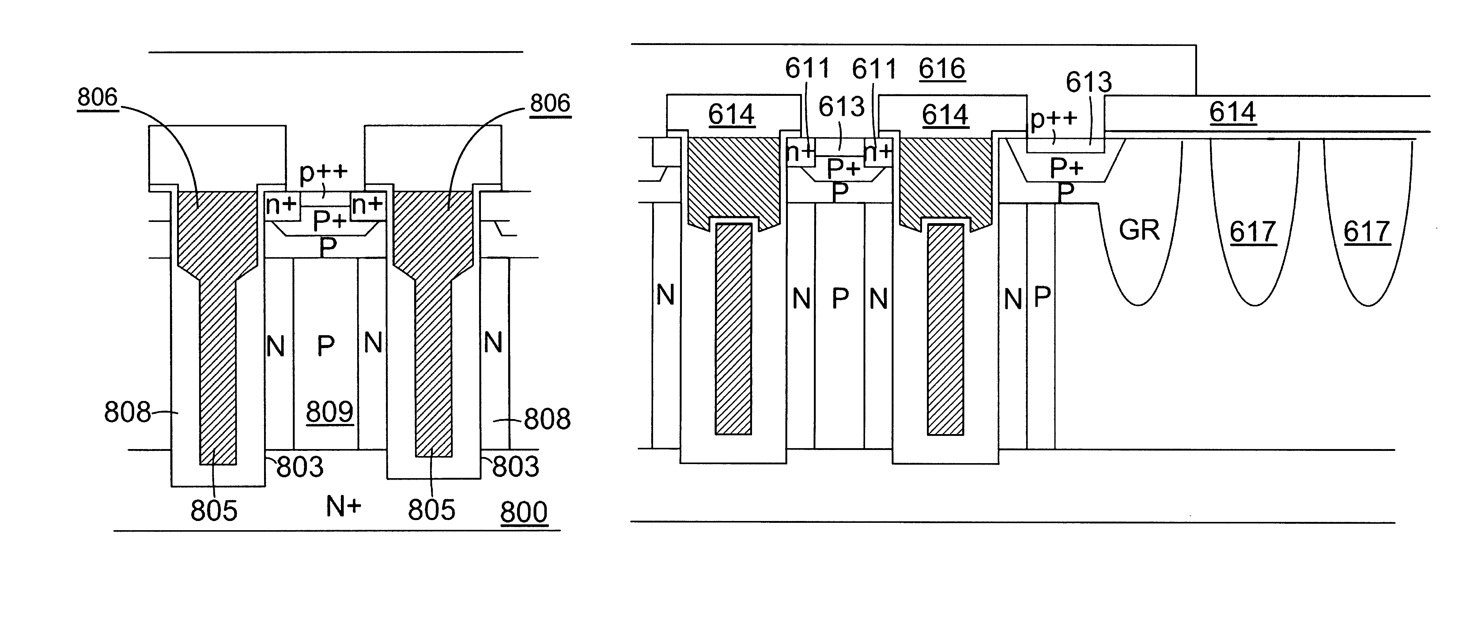
[0027]Please refer to FIG. 2A for a preferred embodiment of this invention where an N-channel super-junction trench MOSFET is formed on an N+ substrate 200 onto which grown an N epitaxial layer 202. A plurality of trenches 203 are formed starting form the upper surface of said epitaxial layer 202 and vertically down extending, not reaching the interface of said substrate 200 and said epitaxial layer 202. Into said trenches 203, doped poly is deposited filling the lower portion of said trenches 203 serving as source electrodes 205 padded by a first insulation layer 204. Into the upper portion of said trenches 203, another doped poly is deposited to serving as gate electrodes 206 onto said source electrodes 205 padded by a second insulation layer 207 having a thinner thickness than said first insulation layer 204. Adjacent to the sidewalls of said trenches 203, N doped region 208 with column shape is formed within said epitaxial layer 202 and in parallel to P doped region 209 with col...


PUM


Abstract

A super-junction trench MOSFET with Resurf Stepped Oxide is disclosed. The inventive structure can apply additional freedom for better optimization and manufacturing capability by tuning thick oxide thickness to minimize influence of charge imbalance, trapped charges, etc. . . . . Furthermore, the fabrication method can be implemented more reliably with lower cost.

Description

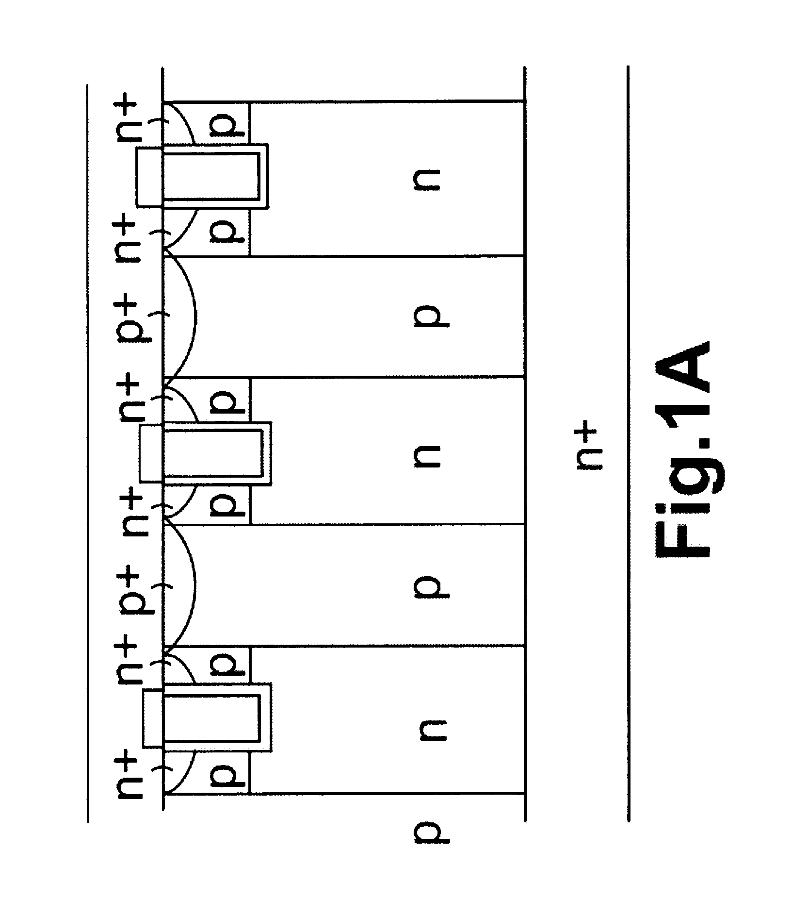
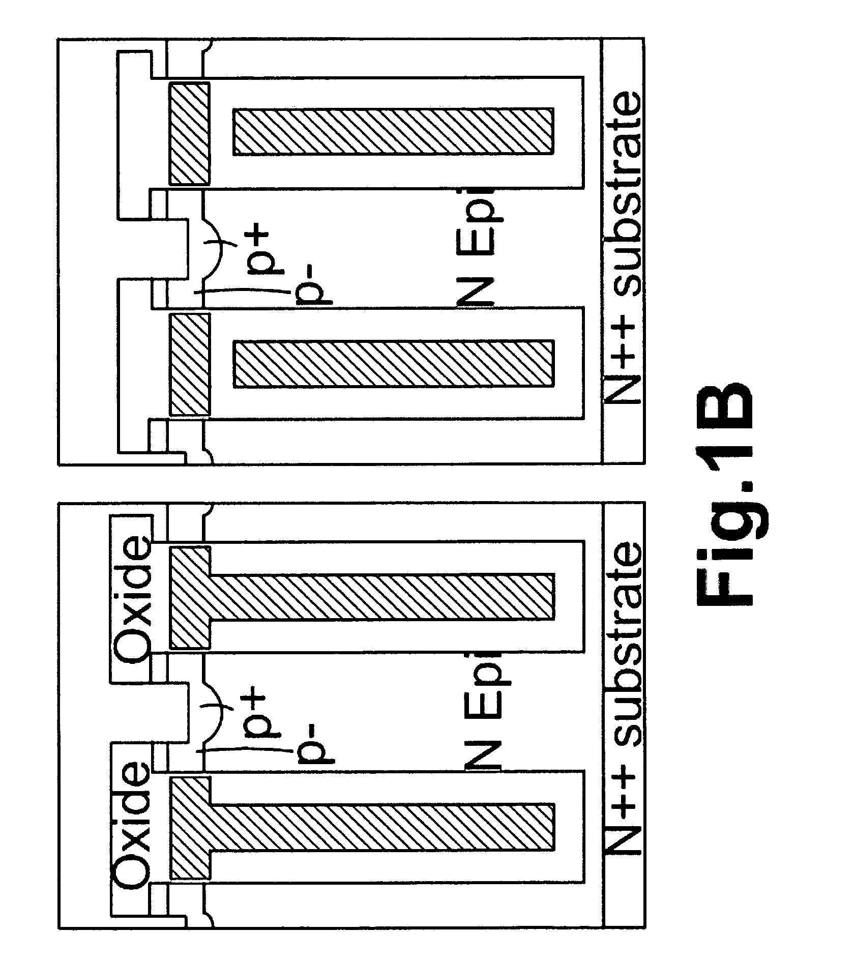
FIELD OF THE INVENTION[0001]This invention relates generally to the cell structure, device configuration and fabrication process of power semiconductor devices. More particularly, this invention relates to a novel and improved cell structure, device configuration and improved process of a super-junction MOSFET.BACKGROUND OF THE INVENTION[0002]Compared to convention trench MOSFET, conventional super-junction trench MOSFET is more attractive due to its higher breakdown voltage and lower specific Rds (drain-source resistance). As is known to all, super-junction trench MOSFET is implemented with p type column structure and n type column structure arranged in parallel and connecting to each other on a heavily doped substrate, however, the manufacturing yield is not stable because it is very sensitive to fabrication process and conditions such as: the p type column structure and n type column structure dopant re-diffusion induced by subsequent thermal processes, trapped charges within the...

Claims


Application Information

Patent Timeline
Patent Type & Authority Patents(United States)
IPC IPC(8): H01L29/66
CPCH01L29/0634H01L29/407H01L29/42368H01L29/66734H01L29/7811H01L29/7813H01L21/26586H01L29/0619H01L29/0878H01L29/1095H01L29/4236H01L29/42376
Inventor HSIEH, FU-YUAN
Owner FORCE MOS TECH CO LTD
Learn More