Flexible nano-imprint stamp

a nano-imprinting and flexible technology, applied in the field of nano-imprinting stamps, can solve the problems of deformation of the stamp, undesirable stretching or distortion of the lithographic pattern of the stamp, applied pressure on the stamp of plachetka et al. and the flexible stamps, etc., to achieve the effect of alleviating, eliminating or mitigating

Active Publication Date: 2011-12-13
NIL TECH APS (DK)
View PDF6 Cites 7 Cited by
  • Summary
  • Abstract
  • Description
  • Claims
  • Application Information

AI Technical Summary

Benefits of technology

[0009]Accordingly, the invention preferably seeks to mitigate, alleviate or eliminate one or more of the above-mentioned disadvantages singly or in any combination. In particular, it may be seen as an object of the invention to provide a flexible NIL stamp that may limit the effect of imperfections in or on the substrate to be imprinted with a lithographic pattern and / or imperfections in or on the stamp and any combinations of such imperfections.
[0012]The invention according to the first and second aspect is particularly but not exclusively advantageous for obtaining a nano-imprinting lithographic stamp capable of limiting the effect of imperfections in or on the substrate to be imprinted with a lithographic pattern and / or imperfections in or on the stamp and any combinations of such imperfections. In particular, the present invention provides a stamp that may apply relatively high imprinting forces during imprinting while still limiting the effect of imperfections. Imperfections may comprise: curvature of substrate and / or polymer film on the substrate, curvature of the pressing tool for pressing the stamp against the substrate, entrapment of air between stamp and substrate, protrusions in the substrate to be imprinted, dust or similar unwanted particles at imprinting sites, isolated defects in the lithographic pattern, limited polymer flow of the polymer to be imprinted, insufficient anti-sticking coating on the stamp, etc.
[0022]The nano-imprinting stamp may be so arranged that the first and the second imprinting sections comprise a first portion with a lithographic pattern, a second portion forming part of the membrane, and a third portion. Beneficially, at least the third portion is encapsulated in a resilient back matrix, i.e. said back matrix may comprise an elastomeric polymer, a gel, a confined fluid, gas or similar. The effect of the resilient back matrix may be to evenly distribute the imprinting force during imprinting.
[0024]The nano-imprinting stamp may comprise sensing means so that the displacement in a direction substantially parallel to an imprinting direction of the imprinting stamp for at least one of the first and the second imprinting sections is detectable by said sensing means. Thus, the position of any displacement may be located resulting in a more efficient manufacturing process.

Problems solved by technology

However, a number of technical problems related to NIL have to be solved first, such as: homogeneity of large imprint areas, sub-micron alignment, error detection, cycle time, and critical dimension control.
However, a problem for stamps made of an elastomeric material is that during imprinting the stamp will be deformed in a direction perpendicular to the imprinting direction due to a relatively high Poisson's ratio of the stamp material.
This may cause an undesirable stretching or distortion of the lithographic pattern of the stamp.
Therefore, the applied pressure on the stamp of Plachetka et al. and the flexible stamps of US2003 / 0017424 are effectively limited to a low range of pressures.
Moreover, relatively large but local imperfections in or on the substrate may influence neighbouring imprinting sections of such a stamp.
However, the stamps of US 2002 / 0132482 suffer from the inherent disadvantage that the bending of the mould / substrate the imprinting will inevitably result in an inhomogeneous imprinting pressure, which may in turn seriously deteriorate the formed lithographic pattern.

Method used


Image

  • Flexible nano-imprint stamp
  • Flexible nano-imprint stamp
  • Flexible nano-imprint stamp

Examples


first embodiment

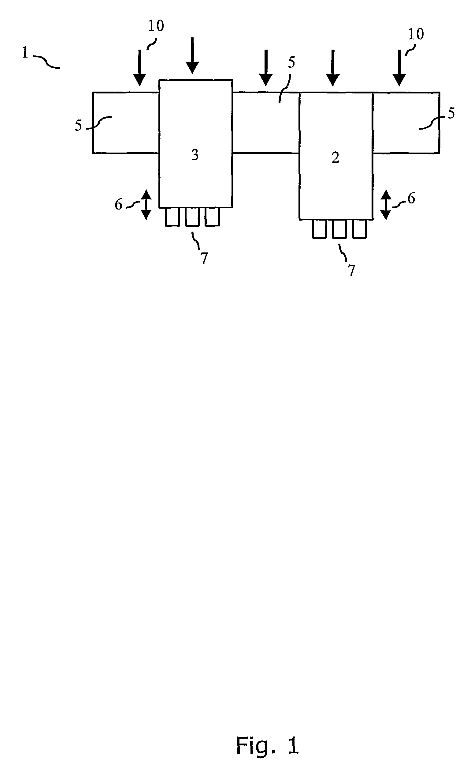
[0038]FIG. 1 shows a cross-sectional view of a nano-imprinting stamp 1 according to the invention. The stamp 1 comprises a first imprinting section 2 and a second imprinting section 3. For reasons of clarity only two imprinting sections 1 and 2 are shown in FIGS. 1 to 3. In the embodiment of FIG. 1, the first and second imprinting sections 2 and 3 are mounted in a base part 5 having appropriate holes for receiving the first and second imprinting sections 2 and 3. The first and second imprinting sections 2 and 3 are mounted in the base part 5 so as to enable that an imprinting force, indicated by the arrows 10, may displace the entire stamp 1 downwards as shown in FIG. 1, while the first and second imprinting sections 2 and 3 are independently displaceable in a vertical direction as indicated by the double-headed arrows 6. This is realised by providing an appropriate friction force at the interfaces between the first and second imprinting sections 2 and 3 and the base part 5. Thus, a...

second embodiment

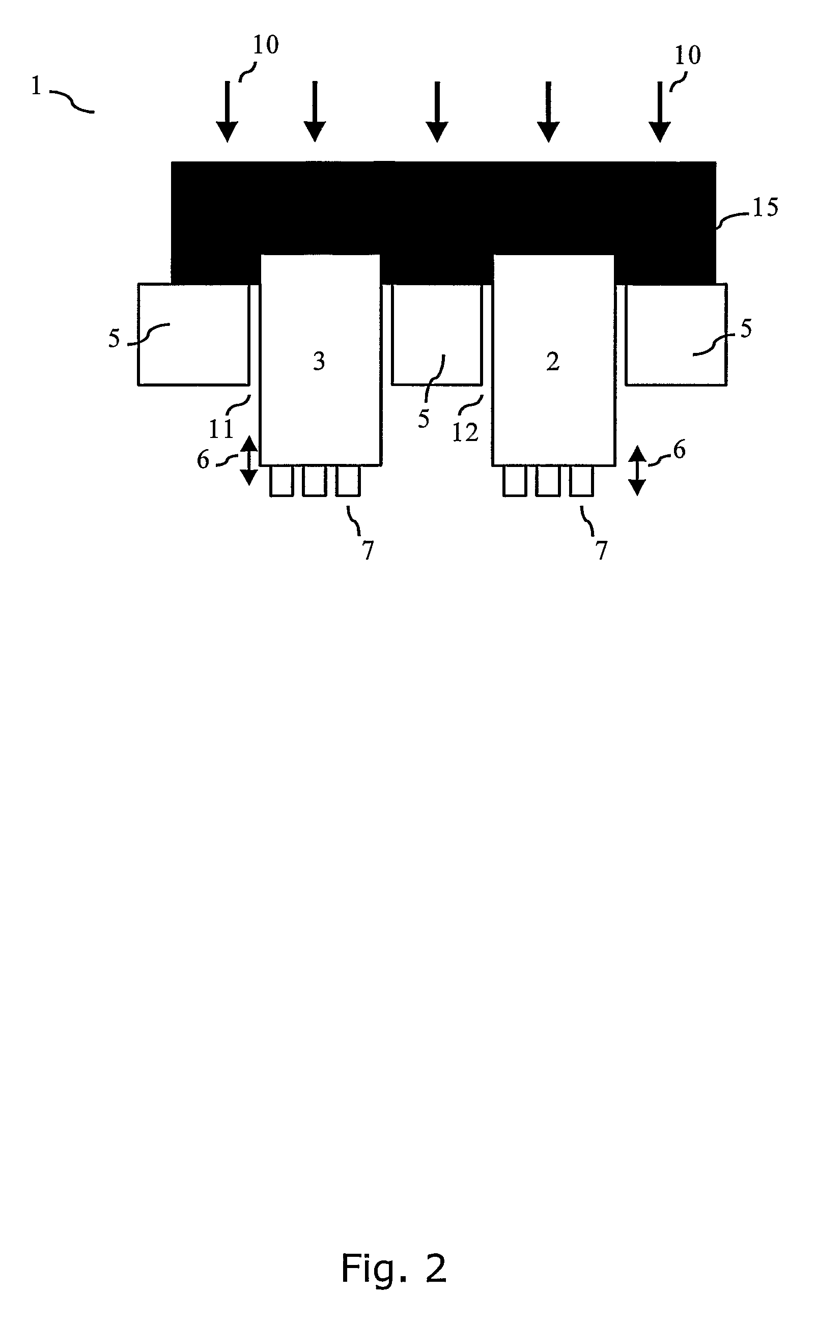
[0039]FIG. 2 shows a cross-sectional view of the nano-imprinting stamp 1 according to the invention. In the embodiment of FIG. 2, the imprinting sections 2 and 3 are received in the corresponding holes 11 and 12 of the base part 5, but there is no direct physical contact between the imprinting sections 2 and 3 and the base part 5. Instead, the upper parts of the imprinting sections 2 and 3 are embedded in a back matrix 15 of an elastomeric material such as PDMS or similar. The back matrix 15 serves the dual purpose of providing a way of transmitting the imprinting force 10 to the imprinting sections 2 and 3 and allowing for the imprinting sections 2 and 3 to be independently displaceable in an imprinting direction of the imprinting stamp 1 as indicated by the arrows 6. The base part 5 serves the purpose of constraining the imprinting sections 2 and 3 in a direction perpendicular to an imprinting direction of the imprinting stamp 1 due to the transversal deformation of the back matri...

third embodiment

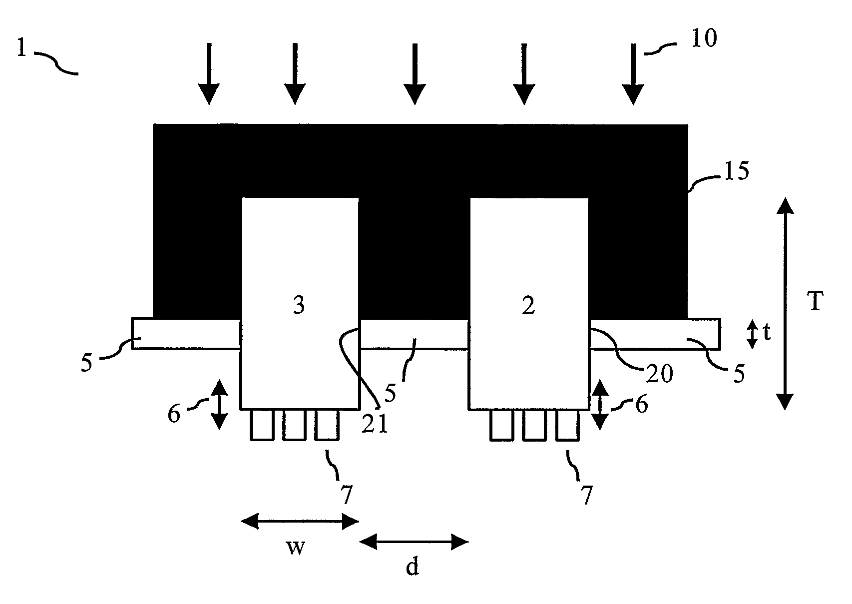
[0040]FIG. 3 shows a cross-sectional view of the nano-imprinting stamp 1 according to the invention. In the embodiment shown in FIG. 3, the imprinting sections 2 and 3 are integrated with the base part 5. Thus, at the interfaces 20 and 21 between the first and second imprinting sections 2 and 3 and the base part 5, the first and second imprinting sections 2 and 3 are either bonded, e.g. by adhesive bonding, anodic bonding, fusion bonding, etc., to the base part 5, or alternatively the base part 5 and imprinting sections 2 and 3 can be manufactured in a single piece of material, e.g. a semiconductor material like Si or similar. In this embodiment, the ability of the first and second imprinting sections 2 and 3 to be independently displaceable in a direction substantially parallel to an imprinting direction of the imprinting stamp 1 is assured by an appropriate design of the magnitude of the thickness t of the base part 5 relative to the thickness T of the imprinting sections 2 and 3 ...


PUM

PropertyMeasurementUnit
displacementsaaaaaaaaaa

Abstract

The present invention relates to a nano-imprinting stamp for imprinting nanometer-sized to mm-sized structures, the stamp (1) having a base part and a first and a second imprinting section (2,3), the first and second imprinting sections having a lithographic pattern (7) intended for imprinting in a receiving substrate. In a first aspect, the first and the second imprinting sections (2,3) are independently displaceable in a direction substantially parallel to an imprinting direction of the imprinting stamp. In a second aspect, the first and the second imprinting sections (2,3) are mechanically weakly coupled in a direction substantially parallel to an imprinting direction of the imprinting stamp. The stamp limits the effect of imperfections in or on the substrate to be imprinted with a lithographic pattern (7) and imperfections in or on the stamp and any combinations of such imperfections by localising the bending of the stamp to the base part (5) in-between the imprinting sections (2,3).

Description

FIELD OF THE INVENTION[0001]The present invention relates to a nano-imprinting stamp for imprinting nanometer-sized to mm-sized structures, the stamp comprises a base part and a first and a second imprinting section, the first and second imprinting sections having a lithographic pattern intended for imprinting in a receiving substrate.BACKGROUND OF THE INVENTION[0002]The drive for miniaturisation to the submicron level within the field of electronics necessitates constant improvements in lithographic processing. Nano-imprint lithography (NIL) is a promising lithographic technique for producing nanometer-sized structures in a parallel process. NIL has been adapted on the International Technology Roadmap for Semiconductors (IRTS) as a potential lithographic technique in order to meet the target of a 32-nm node in 2013. However, a number of technical problems related to NIL have to be solved first, such as: homogeneity of large imprint areas, sub-micron alignment, error detection, cycl...

Claims


Application Information

Patent Timeline
Patent Type & Authority Patents(United States)
IPC IPC(8): B29C59/00
CPCB41F17/001B81C99/009
Inventor NIELSEN, THEODORKRISTENSEN, ANDERSHANSEN, OLE
Owner NIL TECH APS (DK)
Why Eureka
Try Eureka