Memory Cache Control Arrangement and a Method of Performing a Coherency Operation Therefor

a control arrangement and memory cache technology, applied in the direction of memory adressing/allocation/relocation, instruments, computing, etc., can solve the problems of small and expensive but fast memory, data discrepancy, and data transfer number between

Inactive Publication Date: 2008-12-04
FREESCALE SEMICON INC
View PDF3 Cites 26 Cited by
  • Summary
  • Abstract
  • Description
  • Claims
  • Application Information

AI Technical Summary

Problems solved by technology

Unfortunately these characteristics tend to be conflicting requirements and a suitable trade-off is required when designing a digital system.
Thus a PC may typically comprise a large, low cost but slow main memory and in addition have one or more cache memory levels comprising relatively small and expensive but fast memory.
Typically, a cache miss does not only result in the processor retrieving data from the main memory but also results in a number of data transfers between the main memory and the cache.
For example, if data is modified in the main memory without corresponding data of the cache memory being updated or designated as invalid data, disastrous consequences may result.
Similarly, if data which has been written to the cache memory is not transferred to the main memory before it is overwritten in the cache or prior to the corresponding locations of the main memory being accessed directly, the data discrepancy may result in errors.
However, generally such coherency operations are complex, time consuming, power consuming and/or require complex hardware thereby increasing cost.
As the

Method used


Image

  • Memory Cache Control Arrangement and a Method of Performing a Coherency Operation Therefor
  • Memory Cache Control Arrangement and a Method of Performing a Coherency Operation Therefor
  • Memory Cache Control Arrangement and a Method of Performing a Coherency Operation Therefor

Examples


Embodiment Construction

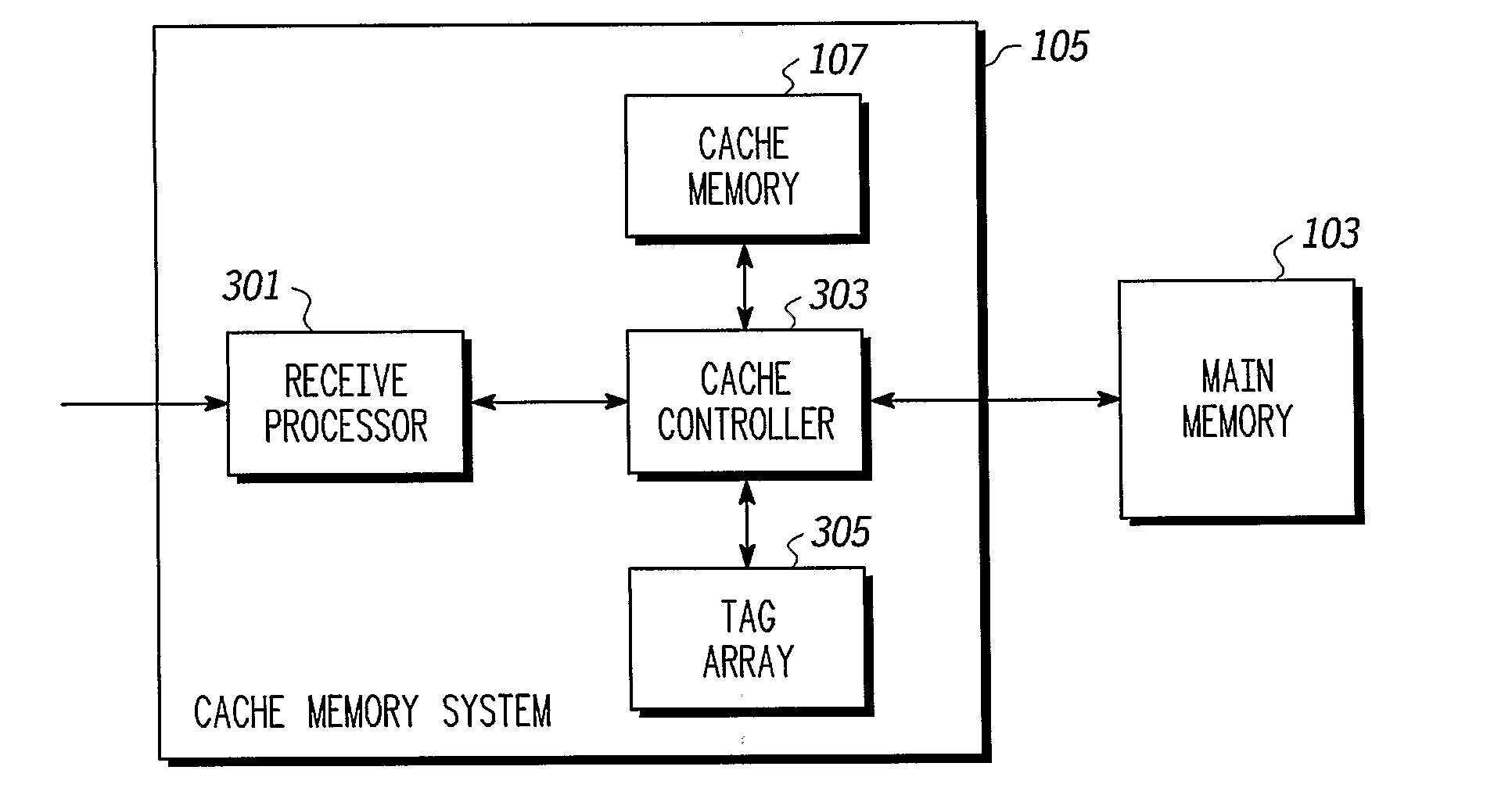
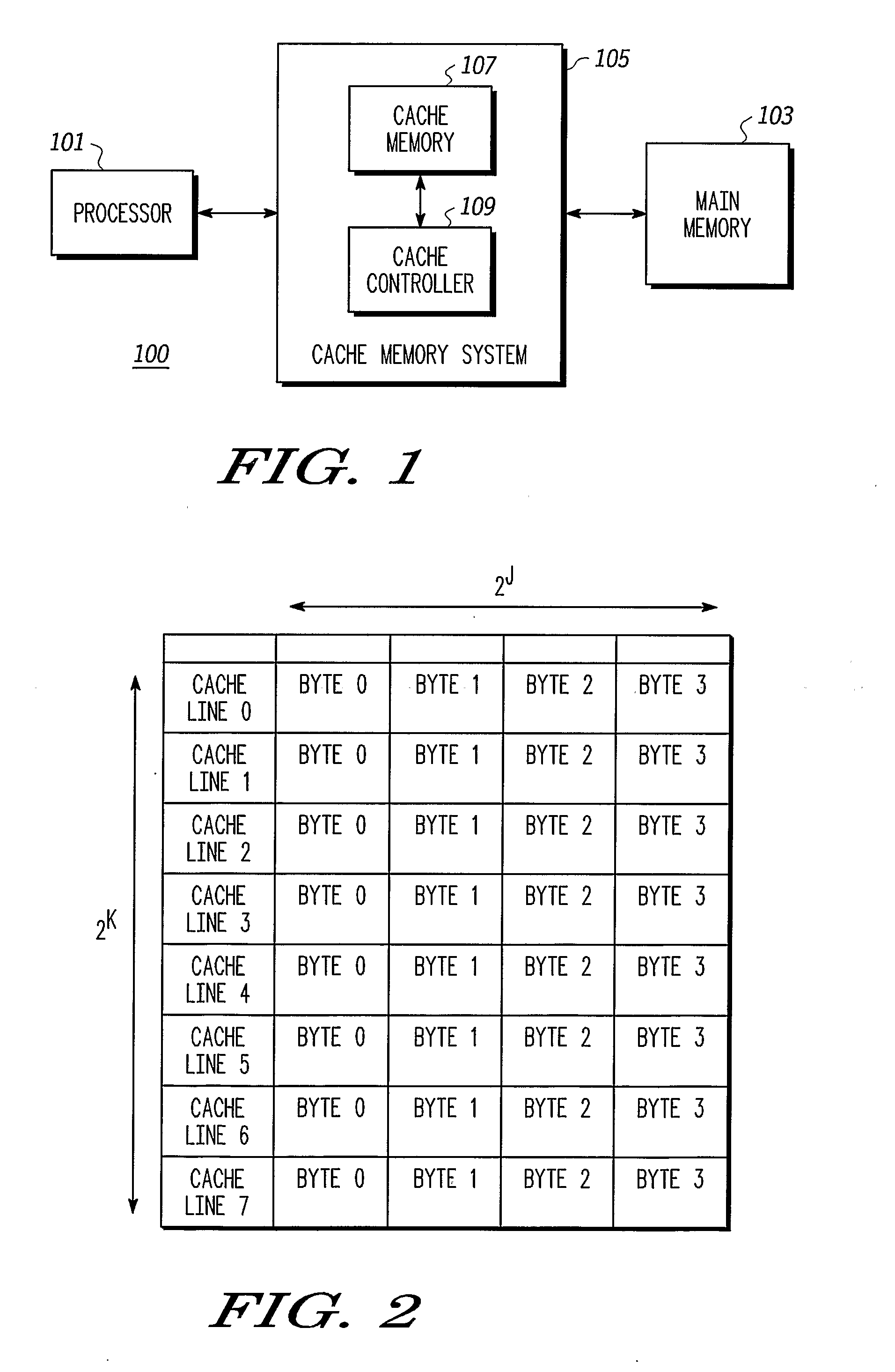
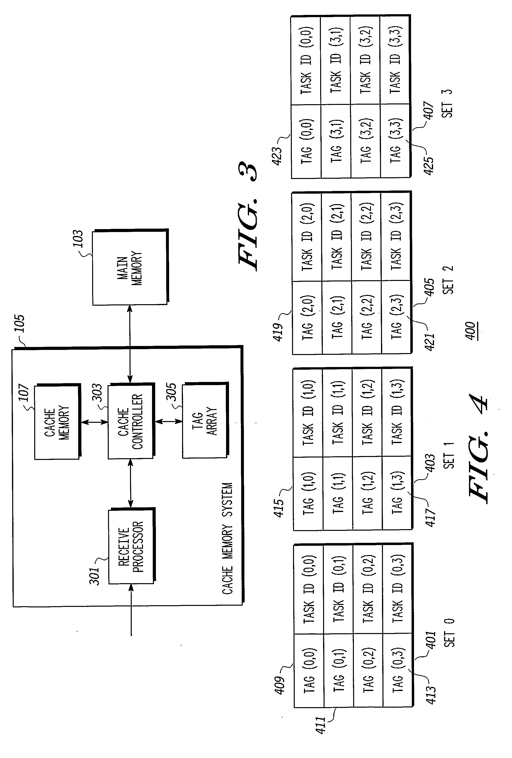
[0029]FIG. 1 is an illustration of a processor system comprising a cache memory system in accordance with an embodiment of the invention.

[0030]A processing system 100 comprises a processor 101 and a main memory 103 which stores instructions and data used by the processor 101 in running applications. The processor 101 may for example be a microprocessor or a digital signal processor and the main memory is in the embodiment dynamic RAM (Random Access Memory). The main memory 103 is relatively large and may for example be of the order of 1 Gbyte. The processor 101 and the main memory 103 are coupled to a cache memory system 105 which together with the main memory 103 forms a hierarchical memory arrangement for the processing system 100.

[0031]The cache memory system 105 comprises a cache memory 107 and a cache controller 109. The cache memory 107 is in the described embodiment a static RAM which is significantly faster than the dynamic RAM used by the main memory 103. However the cache ...


PUM


Abstract

A memory cache control arrangement for performing a coherency operation on a memory cache comprises a receive processor for receiving an address group indication for an address group comprising a plurality of addresses associated with a main memory. The address group indication may indicate a task identity and an address range corresponding to a memory block of the main memory. A control unit processes each line of a group of cache lines sequentially. Specifically it is determined if each cache line is associated with an address of the address group by evaluating a match criterion. If the match criterion is met, a coherency operation is performed on the cache line. If a conflict exists between the coherency operation and another memory operation the coherency means inhibits the coherency operation. The invention allows a reduced duration of a cache coherency operation. The duration is further independent of the size of the main memory address space covered by the coherency operation.

Description

FIELD OF THE INVENTION[0001]This invention relates to a memory cache control arrangement and a method of performing a coherency operation therefor.BACKGROUND OF THE INVENTION[0002]Digital data processing system are used in many applications including for example data processing systems, consumer electronics, computers, cars etc. For example, personal computers (PCs) use complex digital processing functionality to provide a platform for a wide variety of user applications.[0003]Digital data processing systems typically comprise input / output functionality, instruction and data memory and one or more data processors, such as a microcontroller, a microprocessor or a digital signal processor.[0004]An important parameter of the performance of a processing system is the memory performance. For optimum performance, it is desired that the memory is large, fast and preferably cheap. Unfortunately these characteristics tend to be conflicting requirements and a suitable trade-off is required wh...

Claims


Application Information

Patent Timeline
IPC IPC(8): G06F12/08G06F12/00G06F12/0804G06F12/0842G06F12/0891
CPCG06F12/0804G06F12/0842G06F12/0891
Inventor PELED, ITAYANSCHEL, MOSHEEFRAT, YACOVELDAR, ALON
Owner FREESCALE SEMICON INC
Why Eureka
Try Eureka