Stacked type semiconductor memory device and chip selection circuit

a semiconductor memory and stacking technology, applied in the field of semiconductor devices, can solve the problems of large number of electrodes, and high cost, and achieve the effects of reducing cost, reducing cost, and reducing cos

Inactive Publication Date: 2011-12-13
PS4 LUXCO SARL
View PDF41 Cites 23 Cited by
  • Summary
  • Abstract
  • Description
  • Claims
  • Application Information

AI Technical Summary

Benefits of technology

[0006]It is an object of the present invention to provide a stacked type semiconductor memory device in which when selecting a desired semiconductor chip among a plurality of stacked semiconductor chips, a plurality of chip identification numbers different from each other can be automatically generated by a plurality of operation circuits connected in cascade, and the desired semiconductor chip can be reliably selected by a unique identification number assigned to each semiconductor chip using the semiconductor chips having the same structure without employing a complicated structure or particular control.
[0008]According to the aspect of the stacked type semiconductor device of the invention, in order to assign chip identification numbers different from each other to the plurality of semiconductor chips, a structure is employed in which the plurality of operation circuits is connected in cascade and a calculated output of each stage is input to a subsequent stage one after another. For example, an input value of the operation circuit of each stage is defined as the chip identification number, so that its equality with the chip selection address is detected by the comparison circuit. Thereby, for example, when the stacked type semiconductor device is turned on, a plurality of chip identification numbers are automatically generated in the plurality of operation circuits according to the connection relation, and complicated control for generating the chip identification number is not required. And, by appropriately setting a function of the operation, the plurality of identification numbers different from each other can be reliably assigned to the plurality of the semiconductor chips. Further, the plurality of the semiconductor chips may have the same structure, and the number of electrodes can be maintained small even when the number of stacked layers increases so as to realize the stacked type semiconductor device with efficient wiring and an advantage in cost.
[0012]In the present invention, said operation circuit may be an increment circuit which performs an operation of adding 1 to an input value. By this, the chip identification numbers different from each other can be reliably assigned to M semiconductor devices with a simple structure.
[0023]As described above, according to the present invention, in order to select a desired semiconductor chip based on chip identification numbers different from each other in a stacked type semiconductor device in which a plurality of semiconductor chips is stacked, a structure is employed in which an operation circuit and a comparison circuit are provided corresponding to each semiconductor chip, the plurality of identification numbers is generated based on a plurality of operation circuits connected in cascade, and the comparison circuit detects its equality with a common chip selection address. By employing such a structure, the chip identification numbers to be assigned to respective semiconductor chips having the same structure are automatically generated without special control, and each chip identification number is determined depending on the operation circuit so that different numbers are reliably assigned. Further, complicated electrode structure for assigning the chip identification number of each semiconductor chip is not required, and thereby realizing the stacked type semiconductor device with efficient wiring and an advantage in cost regardless of an increase in the number of stacked layers.

Problems solved by technology

Construction of the semiconductor memory using a single semiconductor chip requires finer microfabrication and the yield deteriorates.
However, in such a structure, it is necessary to separately form the connection paths for the selection signals, the number of which is the same as that of stacked layers, and thus when stacking a large number of semiconductor chips, the complicated stacked structure having a large number of electrodes is needed and the production cost increases.

Method used


Image

  • Stacked type semiconductor memory device and chip selection circuit
  • Stacked type semiconductor memory device and chip selection circuit
  • Stacked type semiconductor memory device and chip selection circuit

Examples


Embodiment Construction

[0034]Embodiments of the invention will be described below with reference to accompanying drawings. In this embodiment, a stacked type semiconductor memory device having a plurality of stacked DRAM chips will be described as an example of a stacked type semiconductor device to which the present invention is applied.

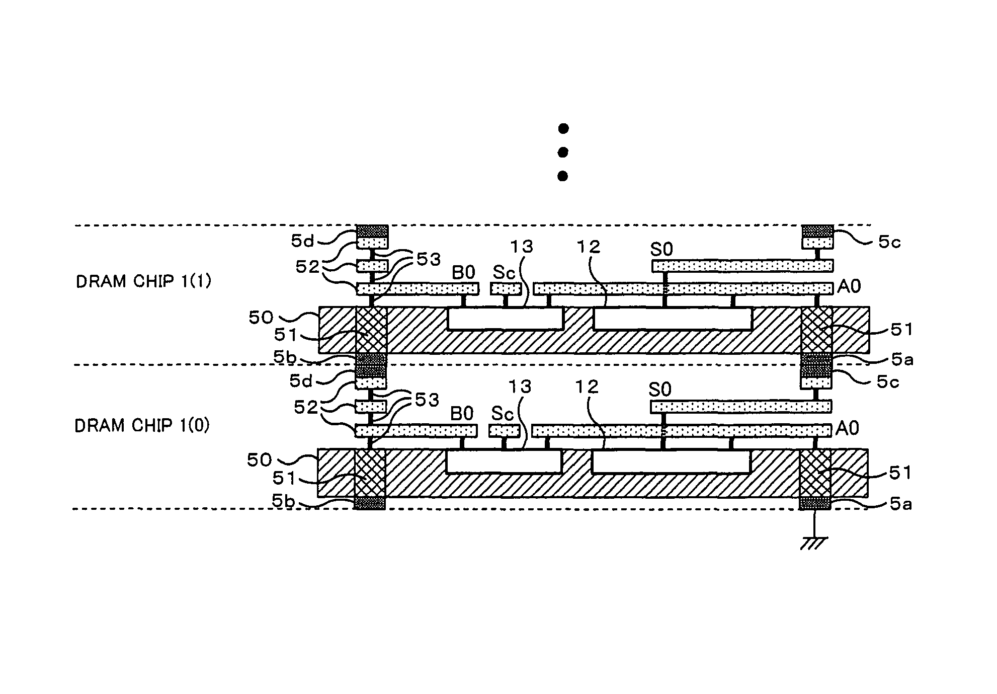
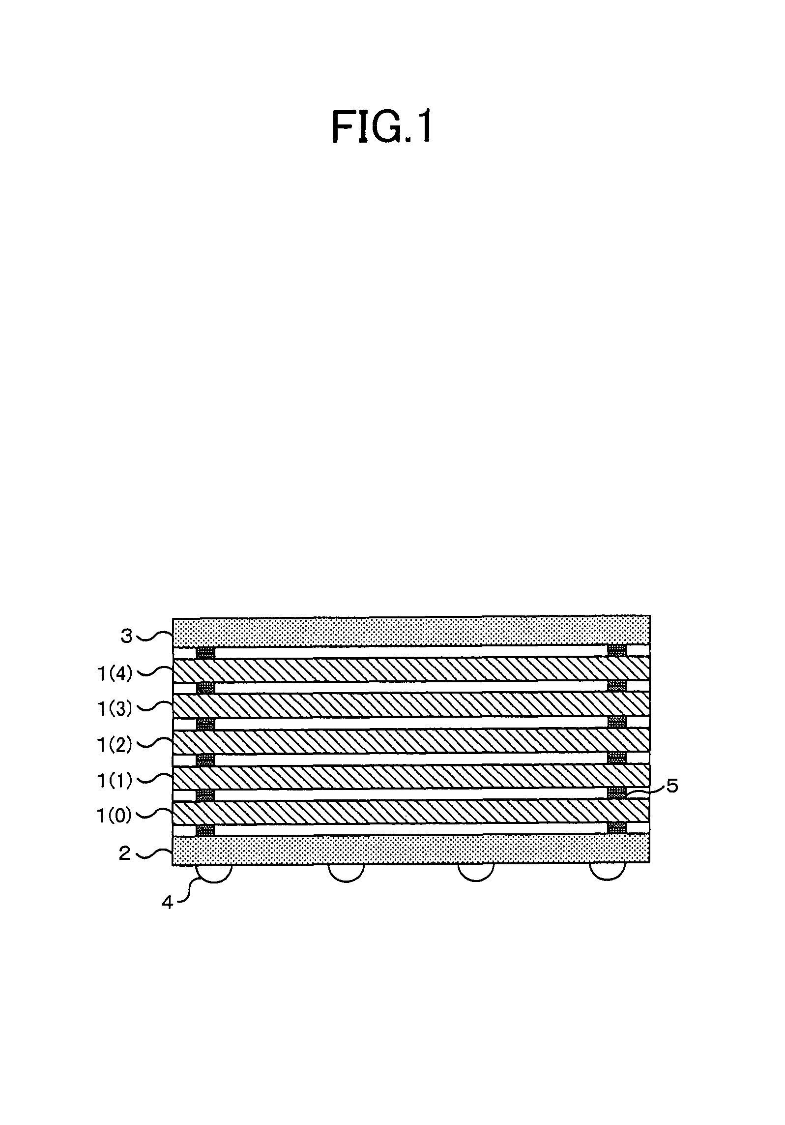
[0035]FIG. 1 is a diagram showing an example of a cross-sectional structure of the stacked type semiconductor memory device of this embodiment. The semiconductor memory device shown in FIG. 1 has a structure in which DRAM chips 1 are stacked in five layers over an interposer board 2 of the lowest layer and an interface chip 3 is stacked thereon. Respective DRAM chips 1 of the first to fifth layers are distinguished from each other by denoting numbers in parenthesis such as DRAM chip 1(0), 1(1), 1(2), 1(3), 1(4) successively.

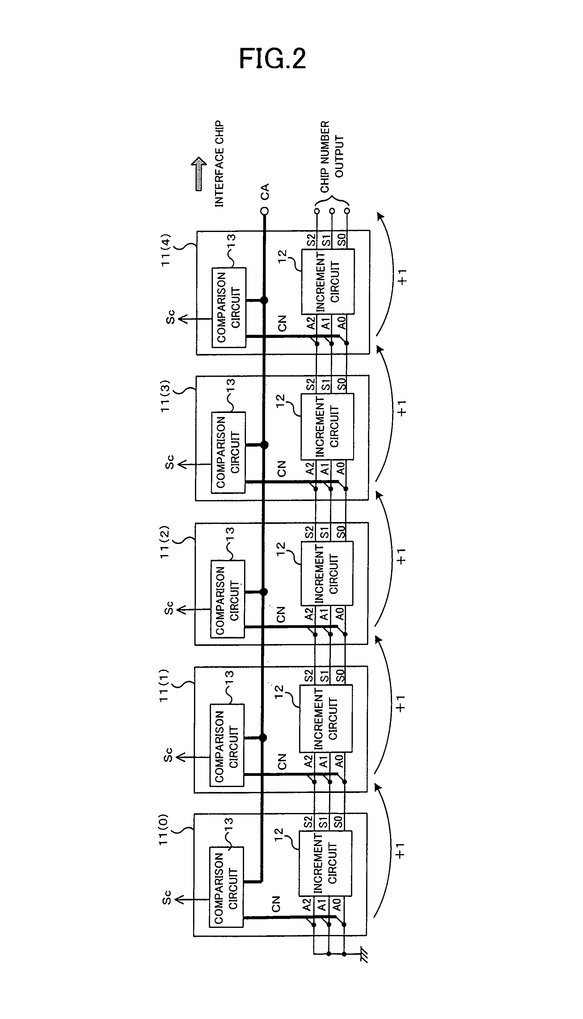
[0036]The five-layer DRAM chips 1(0) to 1(4) have the same storage capacity and the same structure and can perform read / write operation by accessing e...


PUM


Abstract

A stacked type semiconductor memory device of having a structure in which a plurality of semiconductor chips is stacked and a desired semiconductor chip can be selected by assigning a plurality of chip identification numbers different from each other are individually assigned to the plurality of semiconductor chips comprising: a plurality of operation circuits which is connected in cascade in a stacking order of the plurality of semiconductor chips and outputs the plurality of identification numbers different from each other by performing a predetermined operation; and a plurality of comparison circuits which detects whether or not each the identification number and a chip selection address commonly connected to each the semiconductor chip are equal to each other by comparing them.

Description

BACKGROUND OF THE INVENTION[0001]1. Field of the Invention[0002]This invention relates to a semiconductor device having a structure in which a plurality of semiconductor chips is stacked and a specific semiconductor chip can be selected, and particularly relates to a semiconductor device in which a unique identification number is assigned to each semiconductor chip in order to select a specific semiconductor chip.[0003]2. Description of the Related Art[0004]Recently, an increase in storage capacity is required for semiconductor memories such as DRAMs. Construction of the semiconductor memory using a single semiconductor chip requires finer microfabrication and the yield deteriorates. Therefore, a stacked type semiconductor device having a structure in which a plurality of semiconductor chips is stacked has been proposed. For example, by employing a 3 dimensional structure in which a plurality of semiconductor chips of the same type is stacked in multiple layers, a small stacked type...

Claims


Application Information

Patent Timeline
Patent Type & Authority Patents(United States)
IPC IPC(8): H01L23/02
CPCG11C5/02G11C5/04H01L25/0657G11C2029/4402H01L2924/01021H01L2224/16145H01L2225/06513H01L2924/15311
Inventor YAMADA, JUNJIIKEDA, HIROAKISHIBATA, KAYOKOINOUE, YOSHIHIKOMIWA, HITOSHIIJIMA, TATSUYA
Owner PS4 LUXCO SARL
Why Eureka
Try Eureka