

Inspection apparatus and method for inspecting electric characteristics of devices formed on target object
a technology of electric characteristics and inspection apparatus, which is applied in the direction of fault location by increasing semiconductor/solid-state device testing/measurement, etc., can solve the problems of affecting the inspection effect of the device, the temperature difference between the wafer and the probe card, and the damage of the device or the probe, so as to improve the reliability, shorten the inspection time, and prevent the damage of the probe card and the target object.
- Summary
- Abstract
- Description
- Claims
- Application Information
AI Technical Summary
Benefits of technology
Problems solved by technology
Method used
Image


Examples
Embodiment Construction
[0025]Hereinafter, an embodiment of the present invention will be described with reference FIGS. 1 to 3.
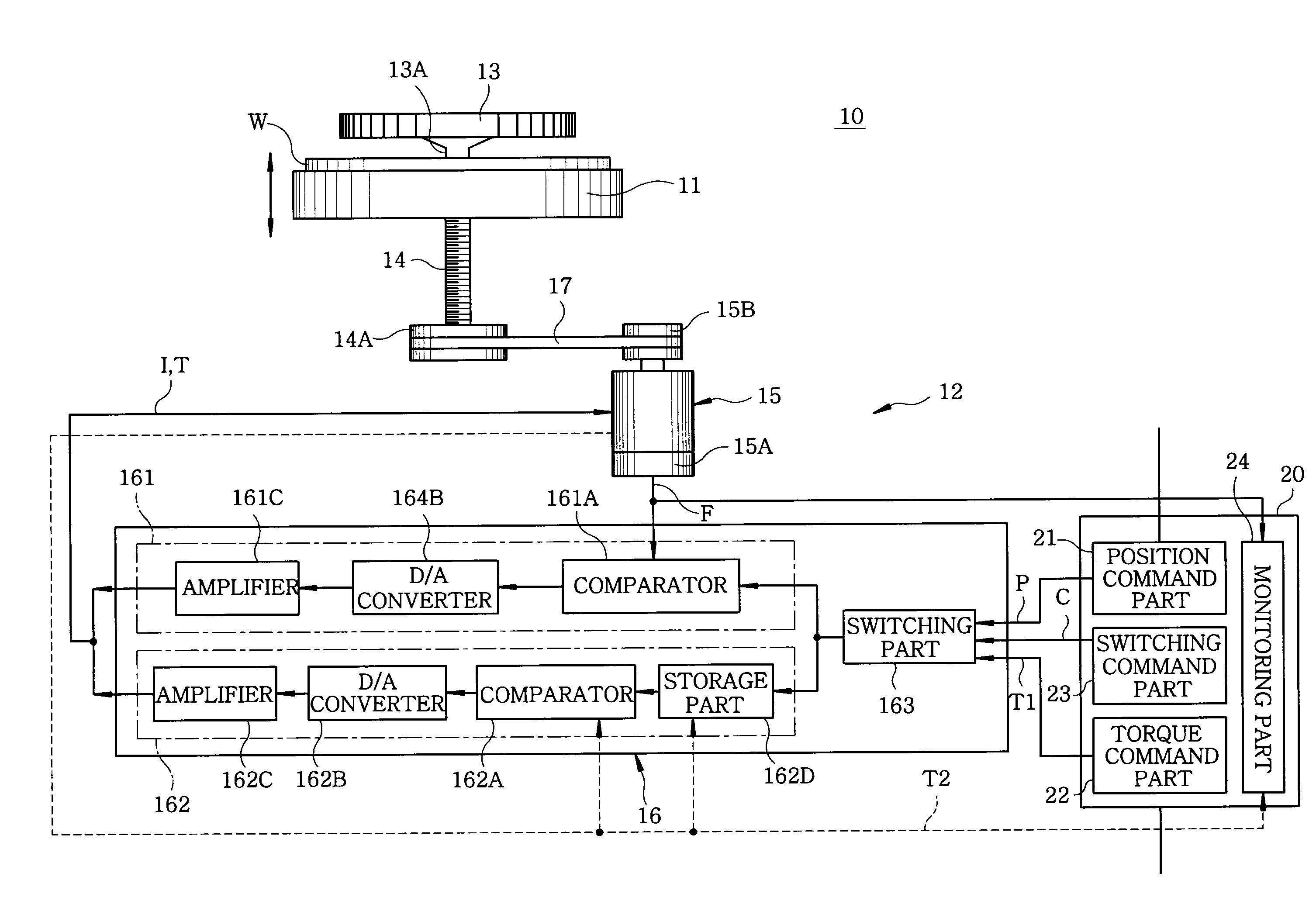
[0026]First, an inspection apparatus of the present embodiment will be described with reference to FIG. 1. As shown in FIG. 1, the inspection apparatus 10 of the present embodiment includes, e.g., a mounting table 11 for mounting thereon a target object (e.g., a wafer) W, the mounting table 11 having therein a temperature controller, a vertical drive mechanism 12 for raising and lowering the mounting table 11, an XY table (not shown) on which the mounting table 11 and the vertical drive mechanism 12 are arranged, a probe card 13 arranged above the mounting table 11 and provided with a plurality of probes 13A and an alignment mechanism (not shown) for aligning the wafer W mounted on the mounting table 11 with the probes 13A of the probe card 13. In a high temperature inspection for example, the vertical drive mechanism 12 is designed to change the current position of the mounting t...
PUM
 Abstract
Description
Claims
Application Information