Inspection method, apparatus and system for circuit pattern

a circuit pattern and inspection method technology, applied in the direction of image enhancement, semiconductor/solid-state device testing/measurement, instruments, etc., can solve the problems of affecting the operation efficiency of the inspection, and requiring one to several hours to fully set the proper inspection conditions. , to achieve the effect of improving the operation efficiency

Inactive Publication Date: 2005-07-19
HITACHI LTD
View PDF2 Cites 24 Cited by
  • Summary
  • Abstract
  • Description
  • Claims
  • Application Information

AI Technical Summary

Benefits of technology

[0022]It is the first object of the invention to provide inspection method, apparatus, and system for a circuit pattern, in which in the case where a defect such as abnormality of a pattern which is generated in a fine circuit pattern, remainder or deposition of a foreign matter, or the like is inspected by using an image formed by irradiating white light, a laser beam, or a charged particle beam, when various conditions necessary for the inspection are set, its operating efficiency can be improved.
[0023]The second object of the invention is to provide inspection method, apparatus, and system for a circuit pattern having an operating picture plane display method or an operating picture plane layout for improving the operability at the time of setting of the inspecting conditions.
[0024]The third object of the invention is to provide inspection method, apparatus, and system for a circuit pattern, in which an inspection time can be reduced and a manufacturing yield can be improved owing to an early investigation of causes of a failure of a semiconductor device.
[0026]First, according to the invention, an inspection target region of an inspection-subject substrate is displayed and a map picture plane which is designated and an image of an optical microscope or an electron beam microscope of a designated region are displayed in parallel, thereby enabling a defect distribution and a defective image to be simultaneously seen.
[0028]Third, according to the invention, tabs showing the item names are sequentially arranged in order of operations, and the tab corresponding to the picture plane which is at present being operated is displayed by a color or a display style which is different from that of the other tabs. Thus, a procedure of the ordinary operations is displayed as a layout and the tab on the picture plane in which parameters are at present being inputted is displayed in a manner different from the tab on each of the other picture planes, thereby enabling the operator to recognize at which stage in the whole operation the present operation is.

Problems solved by technology

On the other hand, since the detection of a defect by the optical image is becoming difficult in association with the reduction in size of a circuit pattern, complication of a shape, and variation of material, a method of inspecting a circuit pattern by using an electron beam image whose resolution is higher than that of the optical image has been proposed.
In the above conventional apparatus, however, there is no disclosure about a procedure for setting the inspecting conditions and an operating method, and it takes one to several hours to fully set the proper inspecting conditions with respect to a wafer whose operation is complicated and which newly becomes a target of inspection.
In a semiconductor manufacturing line, since a pattern inspection is executed with regard to a plurality of products (namely, a plurality of circuit pattern layouts) and a plurality of steps (namely, a plurality of materials and a plurality of detailed circuit pattern shapes), it is necessary to set a large number of inspecting conditions, so that there is a problem that it takes an extremely long time for various operations in the inspection, particularly, for the inspecting condition setting operations.
According to such a method, however, although there is a disclosure about the signal transmission and reception, there is not a disclosure regarding the operability and a data structure for parameters with respect to a complicated inspection apparatus in which the number of input parameters is large.
For example, when many parameters are sequentially inputted and set, although an operating picture plane is sequentially switched in accordance with the input, the operator cannot know the switching order and items which are switched.
There are also problems such that when the data which has already been inputted is confirmed again or inputted, the present picture plane cannot be returned to the previous picture plane or, since the present input stage is obscure, the layer of the picture plane to be returned is unknown, so that the present picture plane cannot be returned to the previous picture plane unless many operations are performed, and the like.
In still another conventional apparatus, although a plurality of parameter input picture planes can be displayed on a workstation for operation by a window format, since a plurality of windows are overlapped and displayed even in such a system, the operator cannot see the information of the picture plane hidden behind the present picture plane, and it is difficult to perform the selecting operation on the picture plane.
Due to the above problems, since it is necessary to form such a large number of input items every kind and step as mentioned above, even if a speed of the inspection itself is high, an efficiency for preparation is low and it takes a long time.
It is, therefore, difficult to apply the inspection to a new product and a new step at an early stage.
When the inspecting conditions are set, since they have to be set by using the inspection apparatus, the inspection time consequently becomes short and the throughput deteriorates.
Even if the inspecting speed is raised, if the subsequent confirmation by the eyes is performed by the same inspection apparatus, a time which can be taken for inspection decreases and, if the operator intends to visually confirm in an apparatus for confirmation by the eyes, it is troublesome to convey the substrate and a method of exchanging data between the apparatuses is complicated, so that there is a problem of deterioration of the throughput.

Method used


Image

  • Inspection method, apparatus and system for circuit pattern
  • Inspection method, apparatus and system for circuit pattern
  • Inspection method, apparatus and system for circuit pattern

Examples


first embodiment

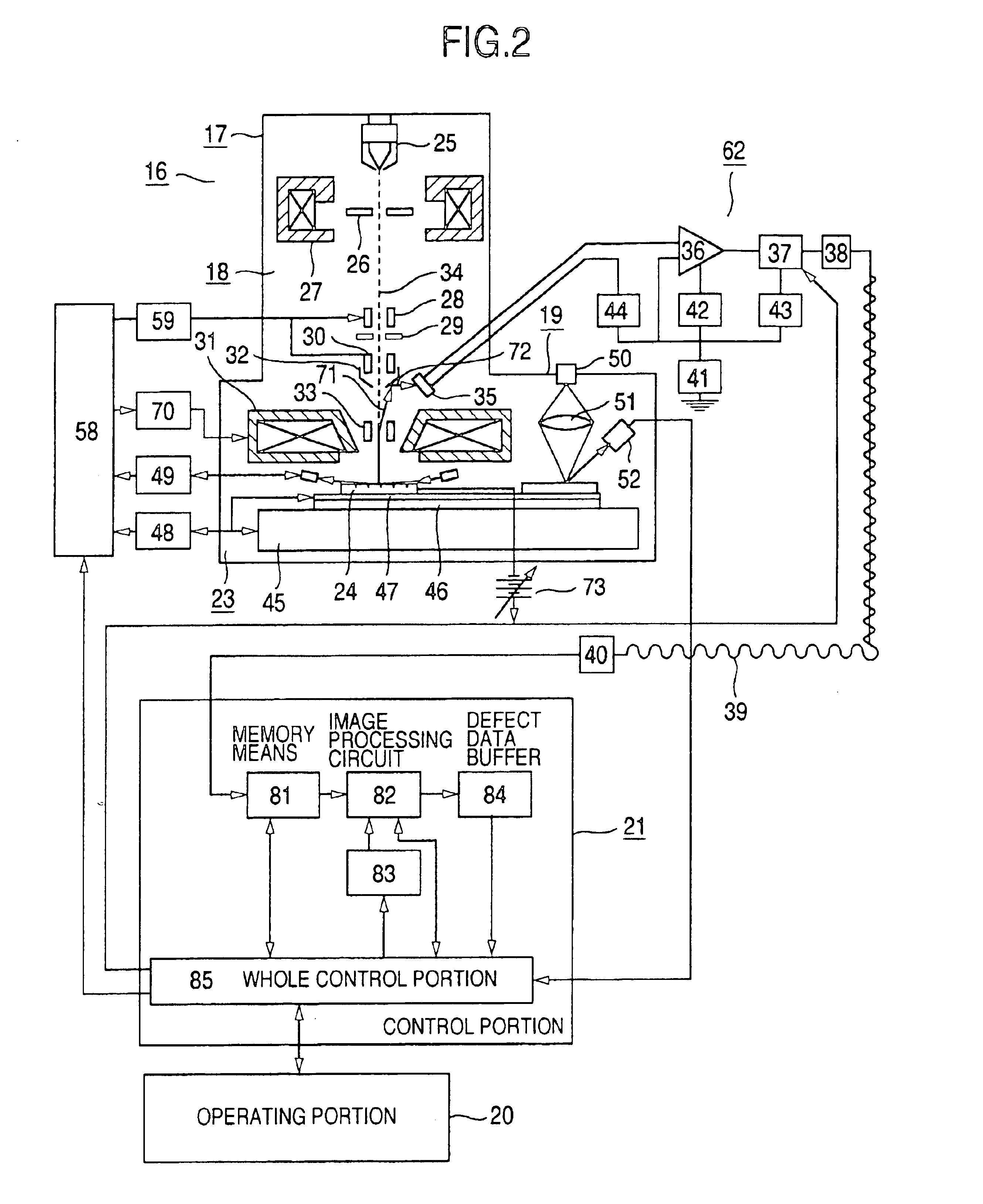
[0072]the invention will be first described hereinbelow with respect to an example of a circuit pattern inspection apparatus in which images obtained by irradiating a charged particle beam, particularly, an electron beam to adjacent circuit patterns on a semiconductor wafer are compared to thereby detect the presence or absence of a defect of the circuit pattern.

[0073]A “cell region” which will be used hereinbelow denotes one unit of a region serving as a target of an inspection and changes in accordance with an inspecting request of the user within a range from a case where it denotes each chip on the wafer to a case where it denotes a specific processing region in the chip. In the invention, an individual region as well as an inspection requesting region of the user is generally called a cell region.

[0074]A construction of the circuit pattern inspection apparatus in the embodiment is shown in FIG. 2. FIG. 2 is a vertical sectional view of the circuit pattern inspection apparatus, ...

second embodiment

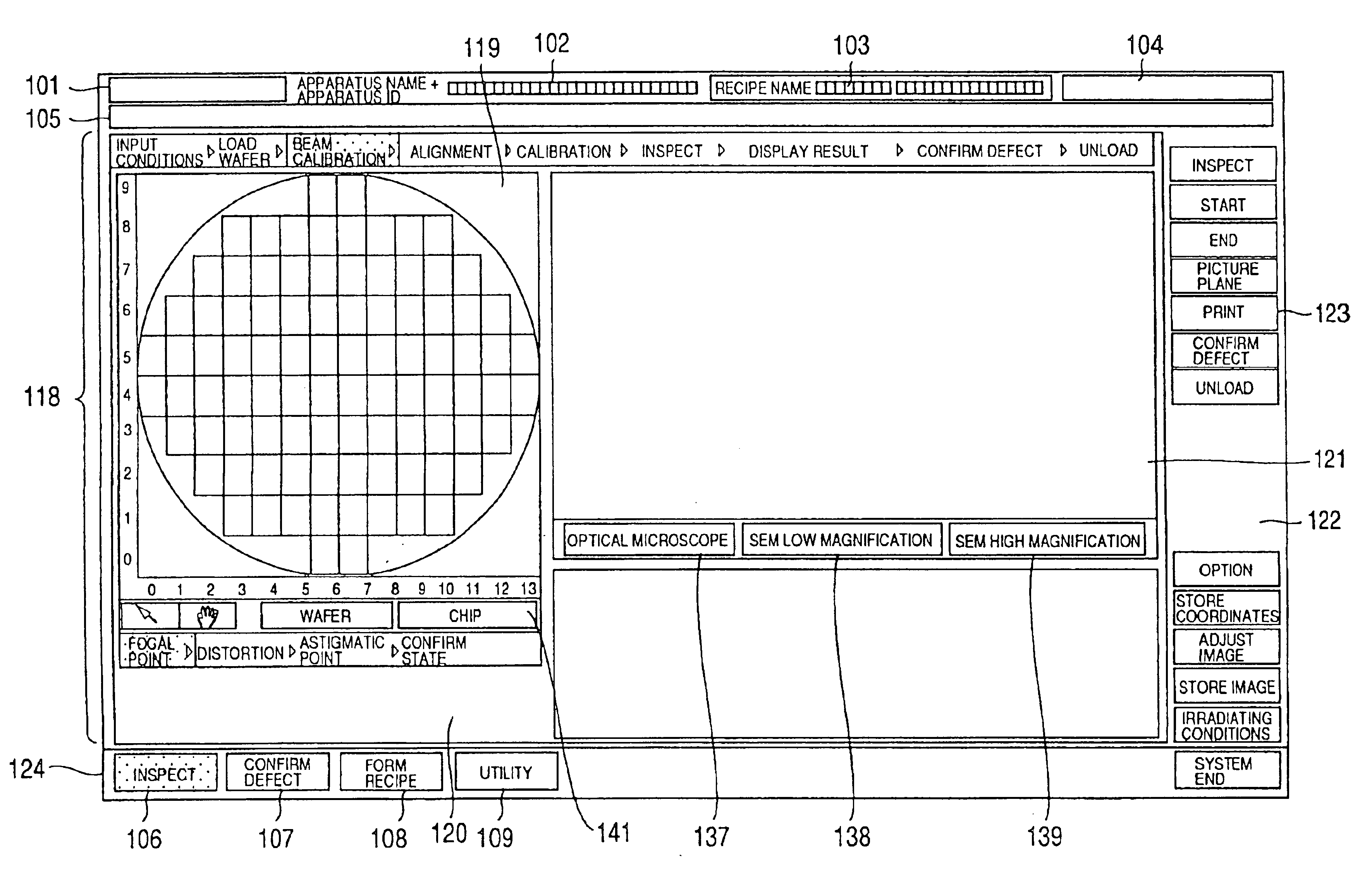
[0104]the invention will now be described hereinbelow. FIG. 6 is a layout diagram of an initial state of a picture plane which is displayed on the monitor 95 shown in FIG. 3. A time display region 101, an apparatus ID display region 102, an inspection target substrate name display region 103, an operator name display region 104, and a message region 105 for displaying various messages are arranged in the top portion of the picture plane. In the lower portion of the picture plane, there are arranged: an “inspect” button 106 to designate the inspecting mode for instructing the start of inspection; a “confirm defect” button 107 to designate the defect confirming mode for instructing the confirmation of a defect; a “form recipe” button 108 to designate the recipe forming mode for instructing the formation of a recipe to preset inspecting conditions; a “utility” button 109 to designate the utility mode for instructing calling of an auxiliary function; and a “system end” button 110 to ins...

third embodiment

[0159]In the inspection, it is necessary to set the cell region as an inspection target region. the invention will now be described hereinbelow.

[0160]FIG. 13 mentioned above shows a map picture plane in a map which is used to set the cell information. Any of an optical microscope image, an SEM type low magnification image, and an SEM type high magnification image can be designated by clicking any of the “optical microscope” button 137, “SEM low magnification” button 138, and “SEM high magnification” button 139. On the picture plane of the cell information, the cell region arranged in a map-in-chip 140 displayed on the left side in FIG. 13 is set while designating it on the image. Further, a cell pitch in the cell region is inputted.

[0161]An “adjust image” button 132, a “store image” button 133, and an “irradiating conditions” button 134 in the option region 130 in FIG. 13 are displayed when the actual picture plane is displayed in an image display portion 156.

[0162]FIG. 15 is a diag...


PUM

PropertyMeasurementUnit
energyaaaaaaaaaa
currentaaaaaaaaaa
widthaaaaaaaaaa

Abstract

Inspection method, apparatus, and system for a circuit pattern, in which when various conditions which are necessary in case of inspecting a fine circuit pattern by using an image formed by irradiating white light, a laser beam, or a charged particle beam are set, its operating efficiency can be improved. An inspection target region of an inspection-subject substrate is displayed, and a designated map picture plane and an image of an optical microscope or an electron beam microscope of a designated region are displayed in parallel, thereby enabling a defect distribution and a defect image to be simultaneously seen. Item names of inspecting conditions and a picture plane to display, input, or instruct the contents of the inspecting conditions are integrated, those contents are overlapped to the picture plane and layer-displayed, and all of the item names are displayed in parallel in a tab format in the upper portion of the picture plane of the contents. When a desired item name is clicked, the picture plane is switched and the contents corresponding to the clicked item name are displayed.

Description

[0001]This application is a division of U.S. patent application Ser. No. 09 / 450,856 filed Nov. 29, 1999, now U.S. Pat. No. 6,476,913, which is incorporate herein by reference in its entirety.[0002]This Application relates to:[0003](1) U.S. application Ser. No. 09 / 258,461, filed Feb. 26, 1999, titled “Convergent Charged Particle Beam Apparatus and Inspection Method Using Same”,[0004](2) U.S. application Ser. No. 09 / 131,383, filed Aug. 7, 1997, titled “Method and Apparatus of an Inspection System Using an Electron Beam”, and[0005](3) U.S. application Ser. No. 08 / 811,511, filed Mar. 4, 1997, titled “Method and Apparatus for Inspection Integrated Circuit Pattern”.[0006]The disclosures of the above applications are hereby incorporated by reference.BACKGROUND OF THE INVENTION[0007]The invention relates to inspection method, apparatus, and system for a fine circuit pattern of a semiconductor device, a photomask, a reticle, a liquid crystal, or the like.[0008]An inspection of a semiconducto...

Claims


Application Information

Patent Timeline
Patent Type & Authority Patents(United States)
IPC IPC(8): G03F7/20G03F1/00G01Q30/02G01Q30/04
CPCG03F7/70616G03F7/7065G06T7/001H01J37/226G03F1/0092G06T2207/30141H01J2237/082H01J2237/2817H01L22/12G03F1/84
Inventor NARA, YASUHIKOMACHIDA, KAZUHISANOZOE, MARIMORIOKA, HIROSHIUSAMI, YASUTSUGUHIROI, TAKASHIHAYAKAWA, KOHICHIITO, MAKI
Owner HITACHI LTD
Why Eureka
Try Eureka