Semiconductor device and manufacturing method thereof

a technology of semiconductor devices and manufacturing methods, applied in semiconductor devices, semiconductor/solid-state device testing/measurement, electrical apparatus, etc., to achieve the effect of high-performance semiconductor devices, reduced yield, and increased chip area

Active Publication Date: 2011-12-27
PANASONIC SEMICON SOLUTIONS CO LTD
View PDF6 Cites 3 Cited by
  • Summary
  • Abstract
  • Description
  • Claims
  • Application Information

AI Technical Summary

Benefits of technology

[0024]The present invention is made to solve the above problems, and it is an object of the present invention to provide a semiconductor device capable of controlling a stress to be applied to a channel in an N-channel region and a channel in a P-channel region and capable of suppressing increase in area and reduction in yield, and a manufacturing method of such a semiconductor device.
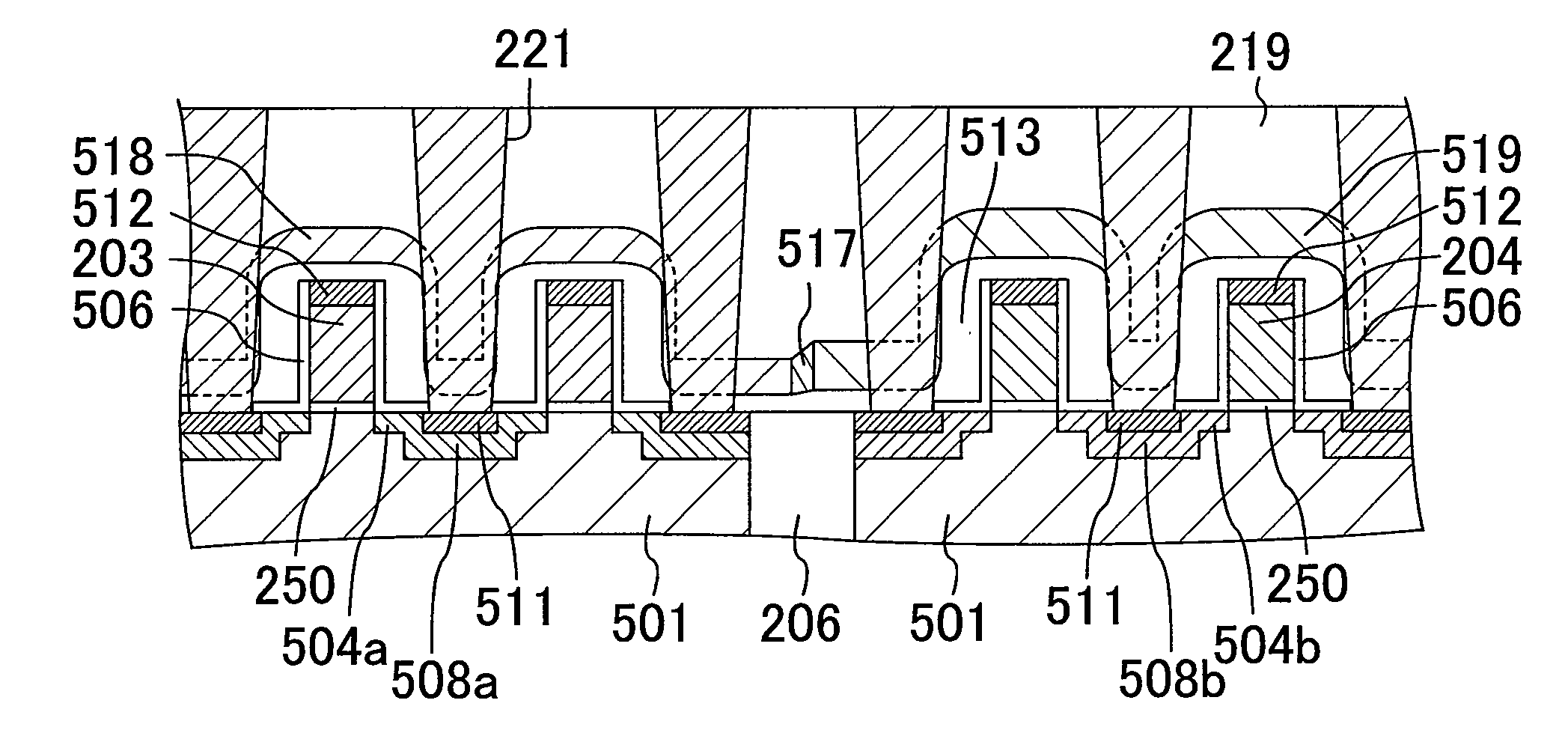
[0026]In this structure, the n-channel contact liner has a shrinkage force and the p-channel contact liner has an expansion force. Accordingly, the channel of the n-channel field effect transistor is subjected to a tensile stress in the gate length direction and the channel of the p-channel field effect transistor is subjected to a compressive force in the gate length direction. The channel mobility can therefore be improved in both the n-channel field effect transistor and the p-channel field effect transistor without using a special material. Especially, since the n-channel contact liner and the p-channel contact liner are formed continuously with each other, the difference in level between the n-channel contact liner and the p-channel contact liner in the np boundary region can be reduced as compared to the conventional semiconductor device, whereby generation of voids can be suppressed. The semiconductor device of the present invention is therefore less likely to have problems such as short-circuit between wirings or between contacts, whereby the yield is improved. Moreover, the yield is not reduced even by forming the contact in the np boundary region, and the width of the np boundary region can be significantly reduced than in the conventional example. As a result, increase in chip area can be suppressed and the degree of freedom in design can be improved.
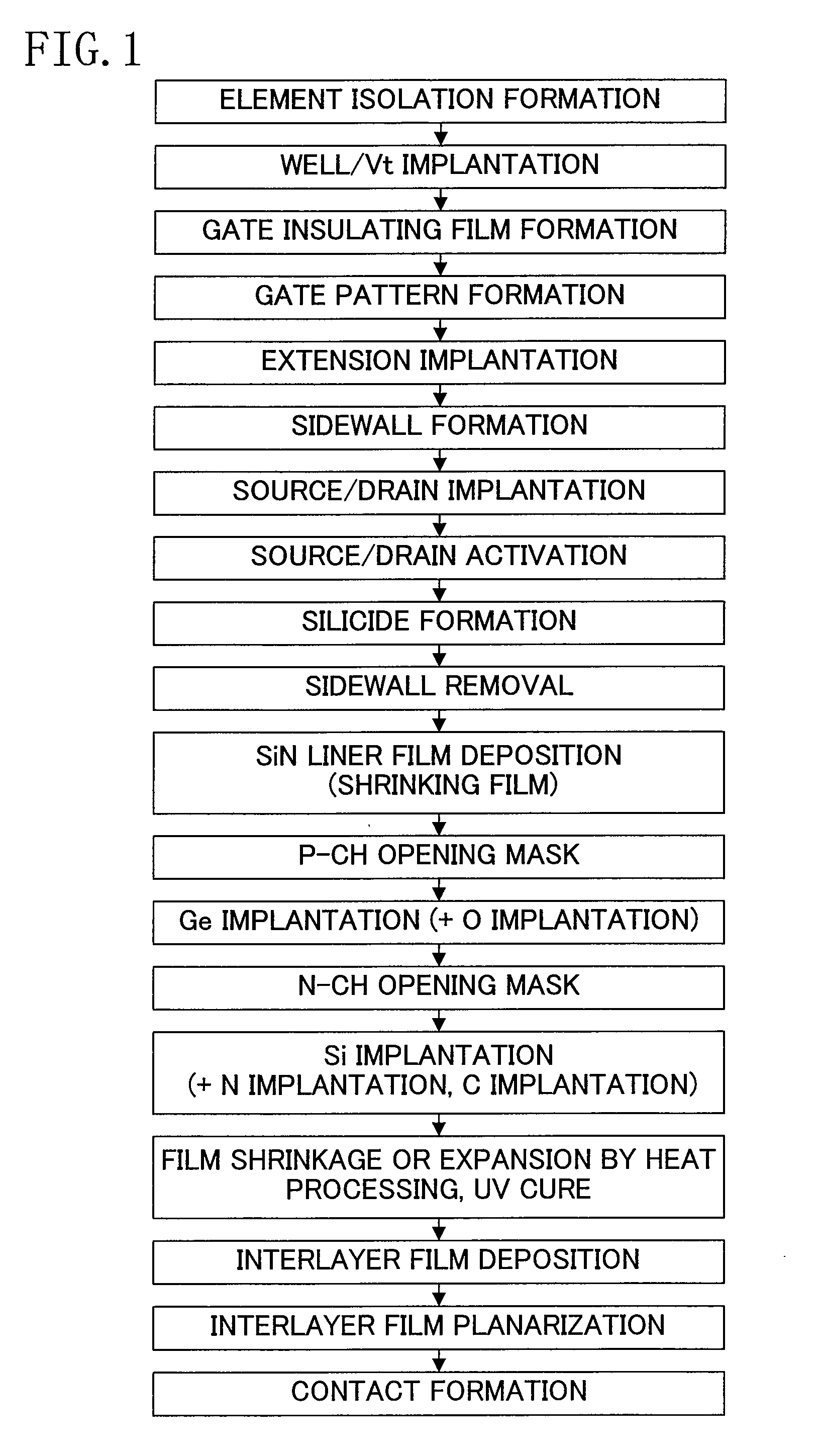
[0028]According to this method, ions of an element having an ionic radius equal to or larger than that of silicon are implanted to the insulating film in the N-channel region in the step (d) to break bonds between the constituent atoms of the insulating film. Since the heat treatment is performed after the bonds between the constituent atoms of the insulating film are broken, the constituent atoms re-bond with each other in a self-aligned manner so as to reduce the film potential, whereby shrinkage of the insulating film can be caused in the N-channel region. As a result, a tensile stress is applied to the channel of the n-channel field effect transistor in the gate length direction, whereby the mobility is improved. Regarding the insulating film in the P-channel region, on the other hand, the bonds between the constituent atoms of the insulating film are first broken in the step (e), and then ions of an element having a higher bonding energy with constituent atoms of the insulating film than that between the constituent atoms are implanted to the insulating film in the P-channel region in the step (f). Therefore, expansion of the insulating film can be caused in the P-channel region. As a result, a compressive force is applied to the channel of the p-channel field effect transistor in the gate length direction, whereby the mobility is improved. Moreover, since the n-channel contact liner and the p-channel contact liner are formed integrally in the manufacturing process, defects such as voids and slits are less likely to be generated in the np boundary region, and the width of the np boundary region can be reduced.
[0031]As has been described above, according to the manufacturing method of the semiconductor device of the present invention, the stress of the contact liner film can be adjusted for n-channel and p-channel after formation of the contact liner. Therefore, the contact liner can be made of one layer, and the contact liner has almost no difference in level in the np boundary region. Therefore, the possibility of increase in chip area and reduction in yield due to increase in the np boundary region is eliminated, and a high performance semiconductor device can be manufactured at low cost.
[0032]Moreover, ion implantation is performed to the contact liner after deposition of the contact liner, and the stress can be increased or reduced by causing shrinkage and expansion of the contact liner. Therefore, the stress to be applied to the channel can be appropriately adjusted according to the transistor type.
[0033]Moreover, there is no overlap of contact liners in the np boundary region. Accordingly, in the case where a silicide layer is formed under the contact liner, the silicide layer is less likely to be damaged in the step of etching the contact liner to form a contact. As a result, increase in silicide resistance is suppressed, whereby a semiconductor device manufactured by the method of the present invention is less likely to suffer from problems such as degradation in transistor characteristics and reduction in yield due to increase in contact resistance and the like.

Problems solved by technology

The area problem of the np boundary region is especially significant in an SRAM (Static Random Access Memory) because the np boundary region occupies a large area in the SRAM.

Method used


Image

  • Semiconductor device and manufacturing method thereof
  • Semiconductor device and manufacturing method thereof
  • Semiconductor device and manufacturing method thereof

Examples


embodiment

[0044]Hereinafter, a method for manufacturing a semiconductor device according to an embodiment of the present invention will be described with reference to the figures.

[0045]FIG. 1 shows a process flow in the method for manufacturing a semiconductor device according to the embodiment of the present invention. FIGS. 2A through 2C, FIGS. 3A through 3C, FIGS. 4A through 4C, and FIGS. 5A through 5C are cross-sectional views showing the method for manufacturing a semiconductor device according to the embodiment of the present invention, and correspond to the process flow of FIG. 1. FIG. 6 is a plan view showing the semiconductor device of the embodiment in the state of FIGS. 5B and 5C. For easy understanding, n-channel gates 203 and p-channel gates 204 are shown by dotted line and sidewalls 505 and an interlayer insulating film 219 are not shown in FIG. 6.

[0046]First, as shown in FIG. 2A, an element isolation region 206 is formed by STI (Shallow Trench Isolation) in a semiconductor subs...


PUM


Abstract

An element larger than silicon is ion-implanted to a contact liner in an N-channel region to break constituent atoms of the contact liner in the N-channel region. An element larger than silicon is ion-implanted to the contact liner in a P-channel region to break constituent atoms of the contact liner, oxygen or the like is ion-implanted. Thereafter, heat treatment is performed to cause shrinkage of the contact liner in the N-channel region to form an n-channel contact liner, and to cause expansion of the contact liner in the P-channel region to form a p-channel contact liner.

Description

CROSS-REFERENCE TO RELATED APPLICATION[0001]This application claims priority from Japanese Patent Application JP2008-031393 filed on Feb. 13, 2008, the disclosure of which application is hereby incorporated by reference into this application in its entirety for all purposes.BACKGROUND OF THE INVENTION[0002]The technology disclosed in the specification relates to a semiconductor device and a manufacturing method thereof. More particularly, the technology disclosed in the specification relates to a semiconductor device having a complementary field effect transistor formed by an n-channel field effect transistor and a p-channel field effect transistor.[0003]With recent improvement of information communication equipments, demand for the processing capability of semiconductor devices such as LSI (Large Scale Integration) has been increasingly strict, and the operation speed of transistors has been increased in response to the demand. Especially a complementary field effect transistor for...

Claims


Application Information

Patent Timeline
Patent Type & Authority Patents(United States)
IPC IPC(8): H01L21/66H01L21/76
CPCH01L21/823412H01L21/823425H01L21/823807H01L29/7843
Inventor KANEGAE, KENSHIYAMADA, MASARU
Owner PANASONIC SEMICON SOLUTIONS CO LTD
Why Eureka
Try Eureka