Complementary-conducting-strip transmission line structure with plural stacked mesh ground planes

a technology of ground planes and junctions, applied in the field of transmission lines, can solve problems such as failure of design rule check (drc), and achieve the effects of enhancing characteristic impedance (zc) and quality factor (q-factor), reducing the requirement of additional chip area, and improving the reliability of circuit design and wafer yield

Inactive Publication Date: 2012-01-31
NAT TAIWAN UNIV +1
View PDF4 Cites 4 Cited by
  • Summary
  • Abstract
  • Description
  • Claims
  • Application Information

AI Technical Summary

Benefits of technology

[0008]One of the purposes of the present invention is to provide a CCS TL structure, which meets manufacturing requirement of metal density, to decrease the requirement of additional chip area and the use of dummy metal, and to improve the wafer yield and circuit design reliability. If any metal layer on circuit design in CMOS process does not meet the minimum metal density requirement, its design rule check (DRC) will be failed. It needs some extra areas for filling some metals to increase the metal density to meet the minimum metal density requirement, and such filling metal is so-called “dummy metal”. Furthermore, the prototype of the CCS TL structure can enhance the characteristic impedance (Zc) and quality factor (Q-factor), while the impact on the slow-wave factor (SWF) is only minimum.

Problems solved by technology

If any metal layer on circuit design in CMOS process does not meet the minimum metal density requirement, its design rule check (DRC) will be failed.

Method used


Image

  • Complementary-conducting-strip transmission line structure with plural stacked mesh ground planes
  • Complementary-conducting-strip transmission line structure with plural stacked mesh ground planes
  • Complementary-conducting-strip transmission line structure with plural stacked mesh ground planes

Examples


embodiment 100

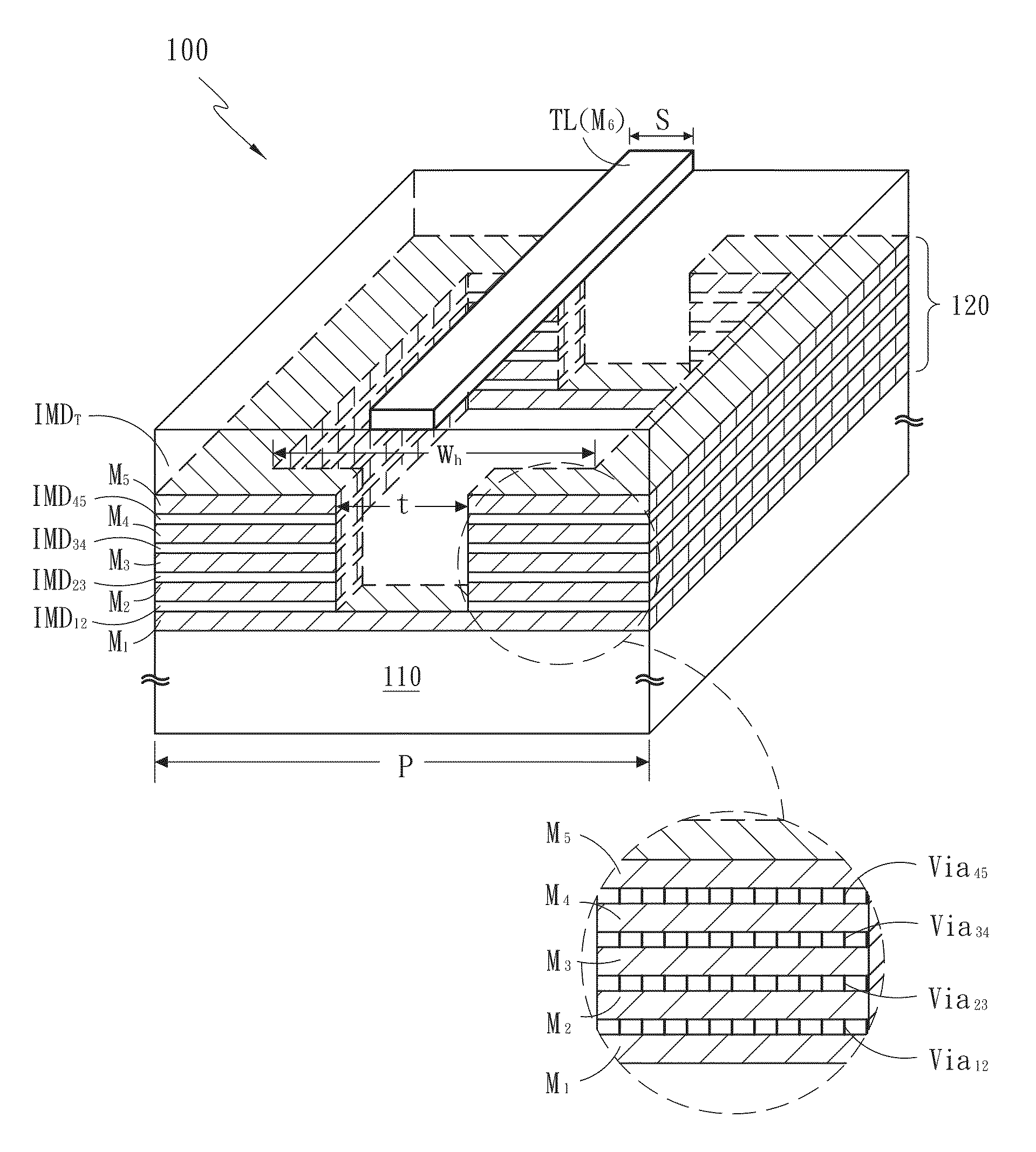
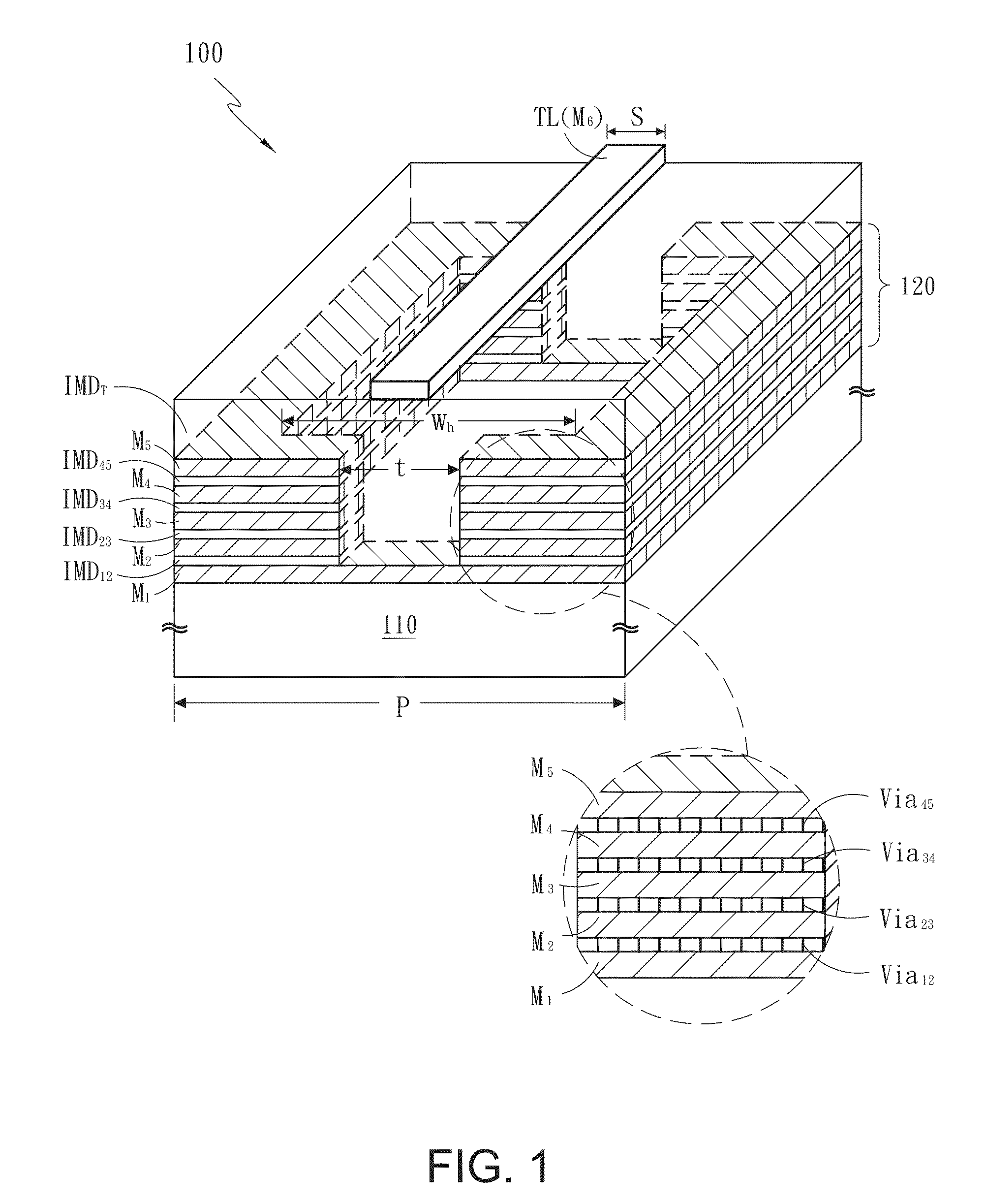
[0024]Referring to FIG. 1, the three-dimensional perspective structure of one preferred embodiment 100 in accordance with the present invention is illustrated. A substrate 110 has a size P (also called a periodicity P). At least one first mesh ground plane M1 and m second mesh ground planes M2, M3, M4, and M5 interlace with m first inter-media-dielectric (thereinafter called IMD) layers IMD12, IMD23, IMD34, and IMD45 (wherein m≧2 and m is a natural number; in the present embodiment, m=4), that is, the first IMD layer IMD12 is between the first mesh ground plane M1 and the second mesh ground plane M2, the first IMD layer IMD23 is between the second mesh ground planes M2 and M3, the first IMD layer IMD34 is between the second mesh ground planes M3 and M4, and the first IMD layer IMD45 is between the second mesh ground planes M4 and M5, to form a stack structure 120 on the substrate 110. Wherein, the first IMD layers IMD12, IMD23, IMD34, and IMD45 respectively have a plurality of vias ...

embodiment 200

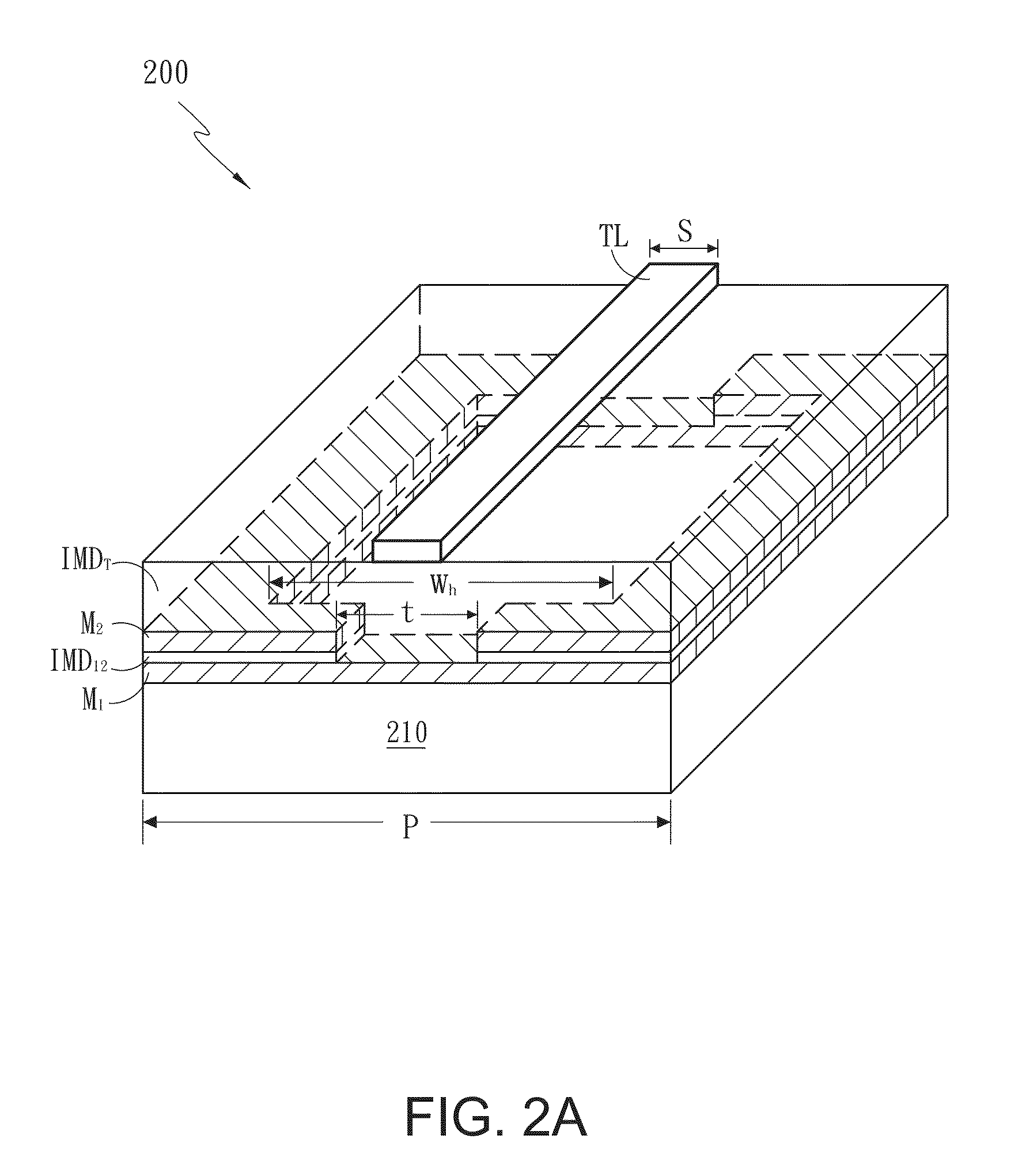
[0027]Referring to FIG. 2A, the three-dimensional perspective structure of another preferred embodiment 200 in accordance with the present invention is illustrated. A substrate 210 has a size P (also called a periodicity P). A first mesh ground plane M1 and a second mesh ground plane M2 sandwich a first IMD layer IMD12 to form a stack structure on the substrate 210. Wherein, the first IMD layer IMD12 has a plurality of vias to connect the first mesh ground plane M1 and the second mesh ground plane M2 to increase the thickness of the mesh ground planes. In the present invention, each mesh ground plane, such as M1 and M2, is a metal layer with an inner slot, and the size of the inner slot (or called mesh slot) is defined as Wh. A second IMD layer IMDT is on the stack structure. A signal transmission line TL with a width S is on the second IMD layer IMDT. Herein, the second mesh ground plane M2 under the signal transmission line TL has at least one slit to form a slit structure with th...

embodiment 260

[0028]Referring to FIG. 2B, the three-dimensional perspective structure of further another preferred embodiment 260 in accordance with the present invention is illustrated. The difference between FIG. 2B and FIG. 2A is that the signal transmission line TL just crosses above one side of the first mesh ground plane M1 and the second ground plane M2. As a result, in FIG. 2B, the second mesh plane M2 under the signal transmission line TL has only one slit to form a slit structure with the slit size t, and this structure can be applied to all embodiments of the present invention. As for the substrate 270 and other elements, such as P, IMD12, IMDT, Wh, S, shown in FIG. 2B, they are the same as the substrate 210 and those elements having the same denotation in FIG. 2A, thus they will not be described again here.

[0029]Referring to FIGS. 3A, 3B, and 3C, the top views for three preferred embodiments 310, 320, and 330 in accordance with the present invention are respectively depicted. In FIG. ...


PUM


Abstract

This invention discloses a complementary-conducting-strip transmission line (CCS TL) structure. The CCS TL structure includes a substrate, at least one first mesh ground plane, m second mesh ground planes having m first inter-media-dielectric (IMD) layers interlaced with and stacked among each other and the first mesh ground plane to form a stack structure on the substrate, a second IMD layer being on the stack structure, and a signal transmission line being on the second IMD layer. Wherein, each first IMD layer has a plurality of vias to correspondingly connect the first and the m second mesh ground planes, therein, m≧2 and m is a natural number, and the m second mesh ground planes under the signal transmission line have at least one slit structure.

Description

BACKGROUND OF THE INVENTION[0001]1. Field of the Invention[0002]This invention generally relates to the field of transmission line structure, and more particularly, to a complementary-conducting-strip transmission line (thereinafter called CCS TL) structure whose capacitive region has at least one slit structure.[0003]2. Description of the Prior Art[0004]Recently, a literature survey shows that there has been renewed interest in the implementation of the microwave / millimeter transmission line based hybrids, which are fabricated by laminated PCB, in monolithic integrated technologies (T. Hirota, A. Minakawa, and M. Muraguchi, “Reduced-size branch-line and rat-race hybrids for uniplanar MMICs,”IEEE Trans. Microwave Theory and Tech., vol. 38, no. 3, pp. 270-275, March 1990; I. Toyoda, T. Hirota, T. Hiraoka, and T. Tokumitsu, “Multilayer MMIC branch-line coupler and broad-side coupler,”IEEE 1992 Microwave and millimeter-wave monolithic circuit symp., pp. 79-82, 1992; K. Hettak, G. A. Mo...

Claims


Application Information

Patent Timeline
Patent Type & Authority Patents(United States)
IPC IPC(8): H01P3/08
CPCH01P3/082
Inventor TZUANG, CHING-KUANGCHIANG, MENG-JUWU, SHIAN-SHUN
Owner NAT TAIWAN UNIV
Why Eureka
Try Eureka