Method of manufacturing high-integrated semiconductor device and semiconductor device manufactured using the same

a manufacturing method and semiconductor technology, applied in the direction of semiconductor devices, basic electric elements, electrical appliances, etc., can solve the problems of difficult to reduce the area of the semiconductor memory device, and achieve the effect of improving the operating characteristic and yield of the semiconductor device and removing alignment errors

Active Publication Date: 2012-02-21
SK HYNIX INC
View PDF7 Cites 2 Cited by
  • Summary
  • Abstract
  • Description
  • Claims
  • Application Information

AI Technical Summary

Benefits of technology

[0007]Various embodiments of the invention are directed to providing a method of manufacturing a semiconductor device including vertical transistors, which is capable of improving the operating characteristic and yield of a semiconductor device by forming bit lines using a conductive material and removing alignment error when the bit lines are formed, and a semiconductor device manufactured using the same.

Problems solved by technology

Accordingly, in the case where a complicated semiconductor memory device is fabricated, it is difficult to reduce the area of the semiconductor memory device because of a number of transistors included in the semiconductor memory device.

Method used


Image

  • Method of manufacturing high-integrated semiconductor device and semiconductor device manufactured using the same
  • Method of manufacturing high-integrated semiconductor device and semiconductor device manufactured using the same
  • Method of manufacturing high-integrated semiconductor device and semiconductor device manufactured using the same

Examples


Embodiment Construction

[0030]Embodiment of the present invention will now be described in detail with reference to the accompanying drawings.

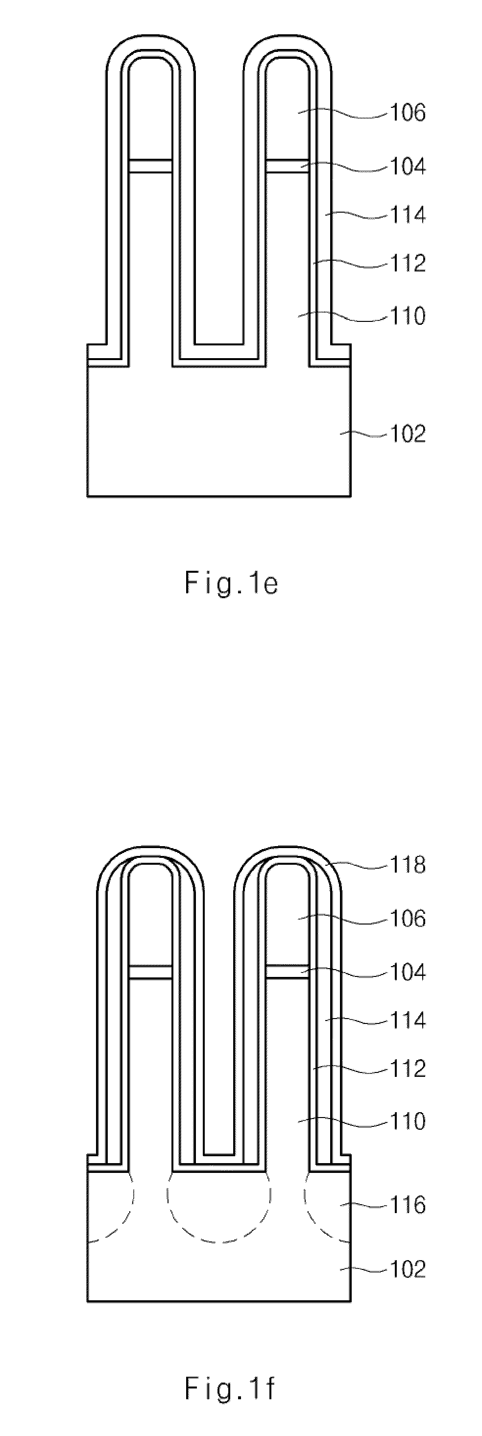
[0031]FIGS. 1a to 1k are plan views and cross-sectional views showing a method of manufacturing a semiconductor device including vertical transistors according to an embodiment of the present invention. In particular, an example in which a vertical transistor is used as a cell transistor included in each of unit cells within a semiconductor memory device is described.

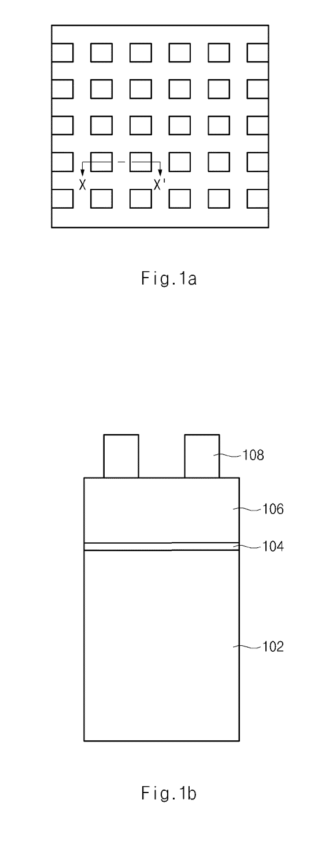
[0032]FIG. 1a is a plan view showing a cell array region within the semiconductor device, and FIG. 1b is a cross-sectional view of the semiconductor device taken along line X-X′ in FIG. 1a.

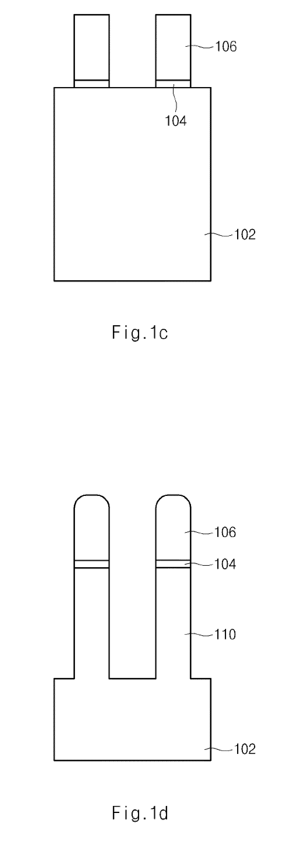
[0033]A pad oxide layer 104 is formed on a semiconductor substrate 102. A hard mask nitride layer 106 is formed on the pad oxide layer 104. A photoresist layer is coated on the hard mask nitride layer 106, and a photolithography process using a mask is then performed, thereby forming a first photoresist layer pattern ...


PUM


Abstract

A semiconductor device comprises a plurality of vertical transistors each comprising barrier metal layers corresponding to source / drain regions in which a conduction region is formed under a channel region having a pillar form, and a bit line comprising a metal layer to connect the plurality of vertical transistors.

Description

CROSS-REFERENCE TO RELATED APPLICATION[0001]The present application claims priority to Korean patent application number 10-2008-0075039, filed on Jul. 31, 2008, which is incorporated by reference in its entirety.BACKGROUND OF THE INVENTION[0002]The present invention relates to a method of manufacturing a semiconductor device and, more particularly, to a method of manufacturing a highly integrated semiconductor device (e.g., vertical transistors) and improving the operating characteristic and yield of the semiconductor device.[0003]In general, a semiconductor is a material classified according to its electrical conductivity and belongs to an intermediate region between a conductor and a nonconductor. The semiconductor has a property that is similar to that of the nonconductor in a pure state, but has an increasing electrical conductivity with the addition of impurities or other control. Such a semiconductor is used to produce semiconductor elements, such as transistors, by adding imp...

Claims


Application Information

Patent Timeline
Patent Type & Authority Patents(United States)
IPC IPC(8): H01L29/78
CPCH01L27/10876H01L29/66666H01L29/7827H10B12/053H01L21/18H01L21/28
Inventor CHO, YOUNG MAN
Owner SK HYNIX INC
Why Eureka
Try Eureka