Printed circuit board

a printed circuit board and circuit board technology, applied in the field of printed circuit boards, can solve the problems of electromagnetic interference (emi) problems that have become more and more of a challenge, noise occurs, and electromagnetic interference (emi) problems that have increased in severity

Active Publication Date: 2012-02-21
MEDIATEK INC
View PDF13 Cites 6 Cited by
  • Summary
  • Abstract
  • Description
  • Claims
  • Application Information

AI Technical Summary

Benefits of technology

[0006]Therefore, a printed circuit board routing with good signal quality and less electromagnetic interference (EMI) effect is desirable.

Problems solved by technology

Along with rapid advances in printed circuit board (PCB) technology, electromagnetic interference (EMI) problems have increased in severity.
When semiconductor devices have higher speeds and higher device densities, noise occurs.
Therefore, for printed circuit board designers, electromagnetic interference (EMI) problems have become more and more of a challenge.
Therefore, the longer current return path results in higher impedance and signal attenuation problems.
The undesired magnetic field increases the coupling coefficient between adjacent signal traces and exacerbates electromagnetic interference (EMI) problems.
A multi-layered PCB, which separates power, signal and ground planes in different layers, may be used to mitigate the aforementioned problems, but adding layers will increase the manufacturing cost of the PCB.

Method used


Image

  • Printed circuit board
  • Printed circuit board
  • Printed circuit board

Examples


Embodiment Construction

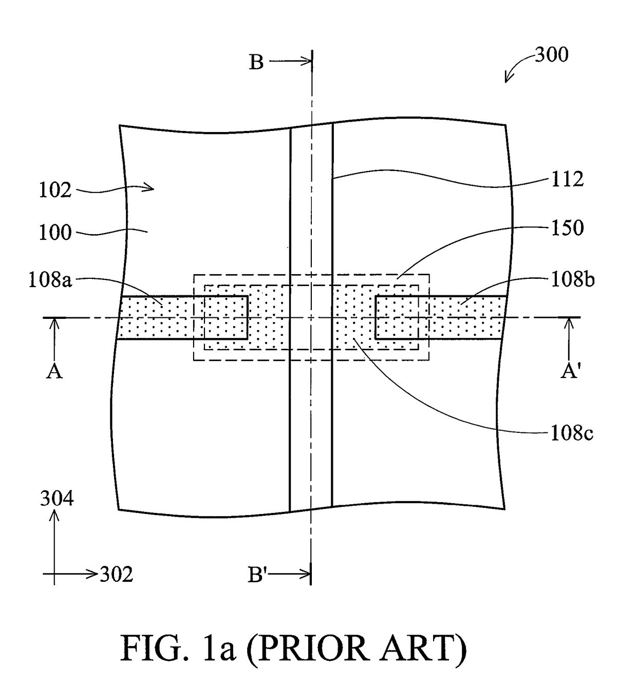
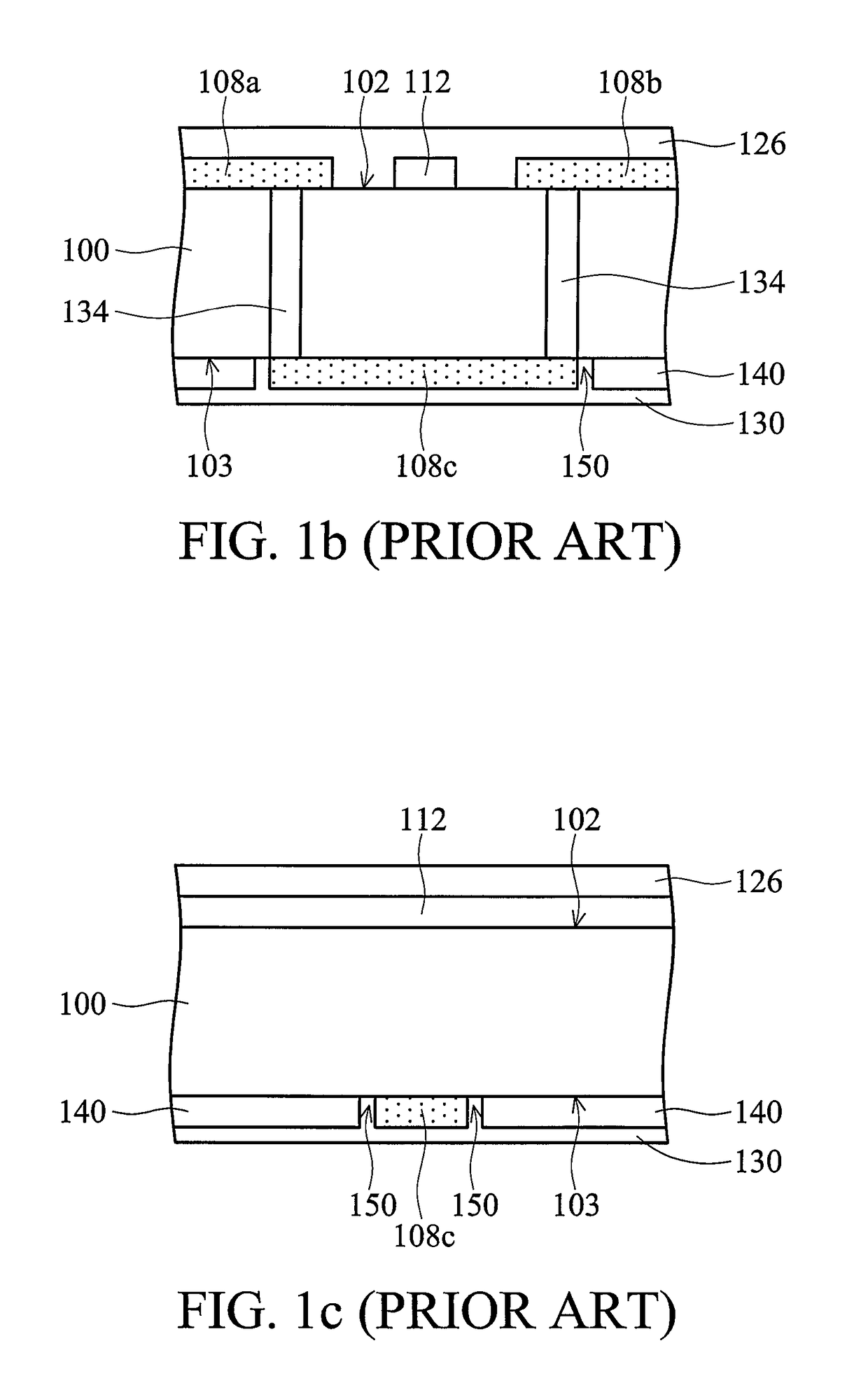
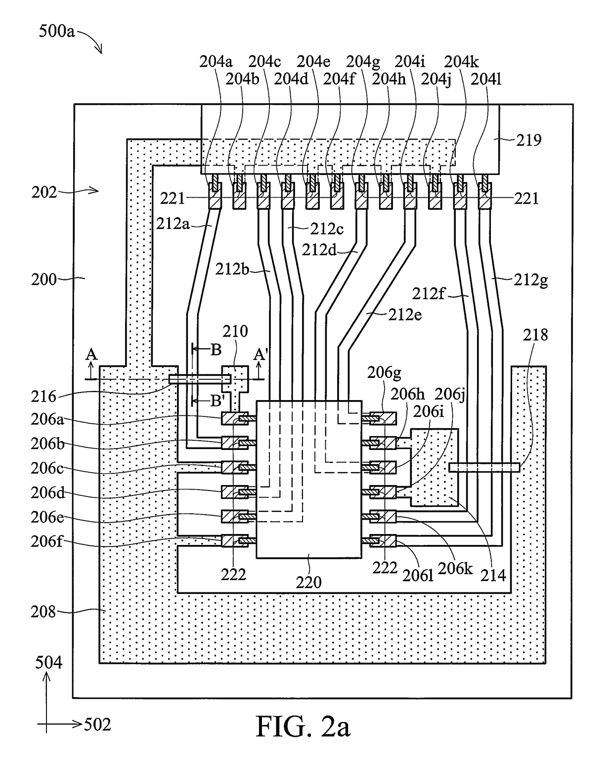
[0023]The following description is of a mode of carrying out the invention. This description is made for the purpose of illustrating the general principles of the invention and should not be taken in a limiting sense. The scope of the invention is best determined by reference to the appended claims. Wherever possible, the same reference numbers are used in the drawing and the description to refer the same or alike parts.

[0024]FIGS. 2a to 2c show one exemplary embodiment of a printed circuit board 500a of the invention. FIG. 2a shows a top view of one exemplary embodiment of the printed circuit board 500a of the invention. In this embodiment, the printed circuit board 500a may comprise a two-layered printed circuit board for leadframe-based semiconductor package chips having a top layer comprising power planes and signal trace, and a bottom layer comprising a ground plane. The printed circuit board 500a comprises a substrate 200 having a top surface 202 and a bottom surface 203 as sh...


PUM


Abstract

A printed circuit board is disclosed. The printed circuit board comprises a substrate having a top surface and a bottom surface. A ground plane is on the bottom surface. A signal trace is on the top surface along a first direction. At least two isolated power planes are on the top surface adjacent to opposite sides of the signal trace, respectively. A conductive connection along a second direction couples to the two power planes, across the signal trace without electrically connecting to the signal trace, wherein the signal trace doesn't pass over any split of the ground plane.

Description

BACKGROUND OF THE INVENTION[0001]1. Field of the Invention[0002]The present invention relates to a printed circuit board (PCB), and in particular to a printed circuit board routing with good signal quality and less electromagnetic interference (EMI) effect.[0003]2. Description of the Related Art[0004]Along with rapid advances in printed circuit board (PCB) technology, electromagnetic interference (EMI) problems have increased in severity. When semiconductor devices have higher speeds and higher device densities, noise occurs. Therefore, for printed circuit board designers, electromagnetic interference (EMI) problems have become more and more of a challenge.[0005]FIG. 1a shows a local top view of the conventional two-layered printed circuit board 300 showing routing of power and signal planes. FIGS. 1b to 1c show cross sections along lines A-A′ and B-B′ of FIG. 1a, respectively. The conventional printed circuit board 300 has a top layer on a top surface 102 of a substrate 100, covere...

Claims


Application Information

Patent Timeline
Patent Type & Authority Patents(United States)
IPC IPC(8): H05K1/11H05K1/14
CPCH05K1/0216H05K3/222H05K2201/0715H05K2201/093H05K2201/09336H05K2201/10363H01L2924/0002H05K2201/10515H05K2201/10689H01L2924/00
Inventor CHEN, NAN-JANGLIN, HONG-CHIN
Owner MEDIATEK INC
Why Eureka
Try Eureka