

Etch methods for semiconductor device fabrication
- Summary
- Abstract
- Description
- Claims
- Application Information
AI Technical Summary
Problems solved by technology
Method used
Image

Examples
Embodiment Construction
[0010]The following detailed description is merely exemplary in nature and is not intended to limit the invention or the application and uses of the invention. Furthermore, there is no intention to be bound by any expressed or implied theory presented in the preceding technical field, background, brief summary or the following detailed description.
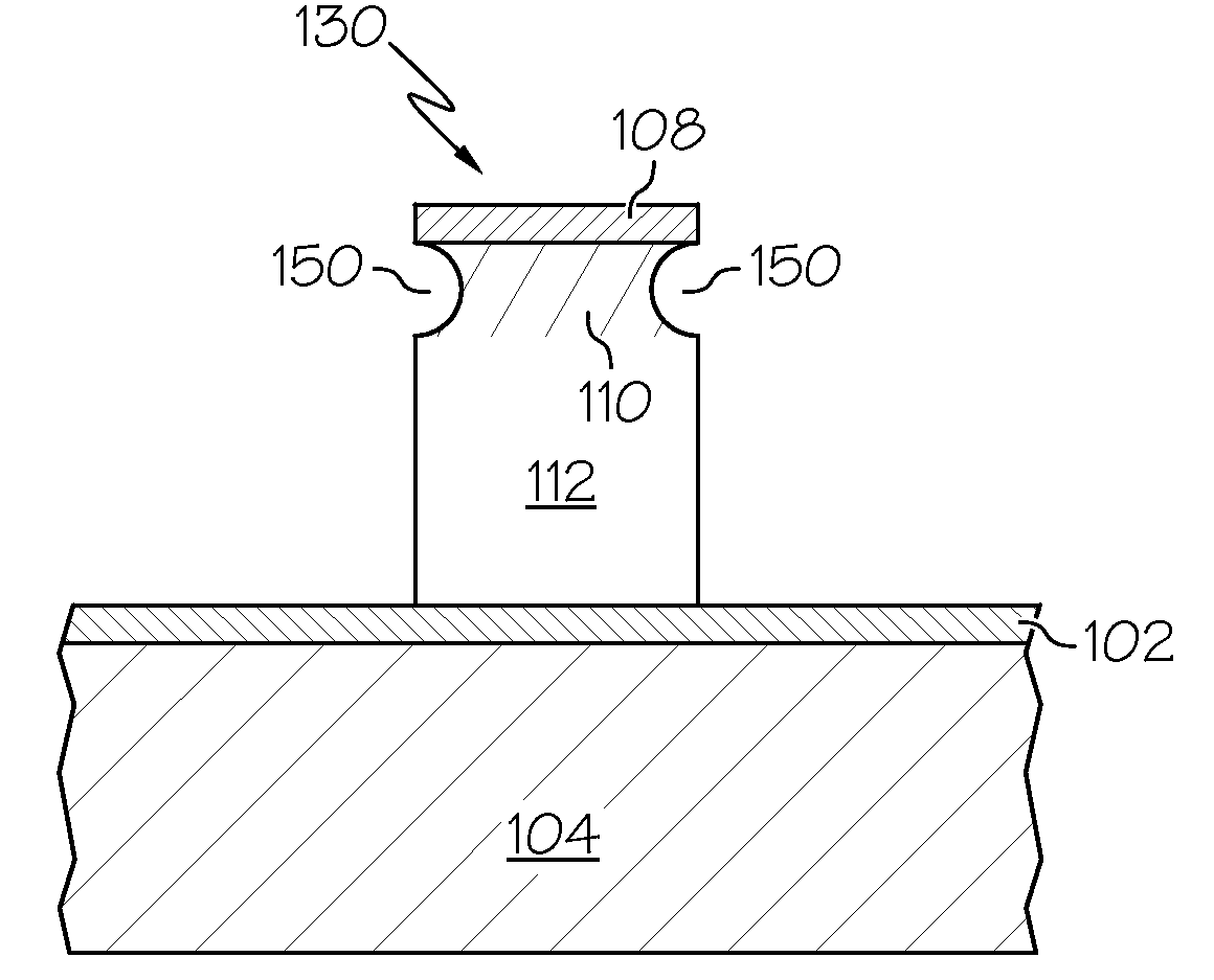
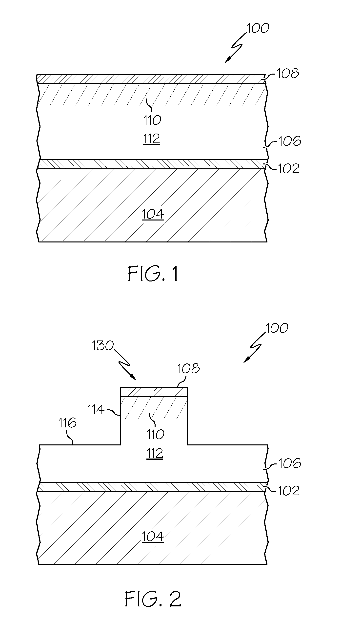
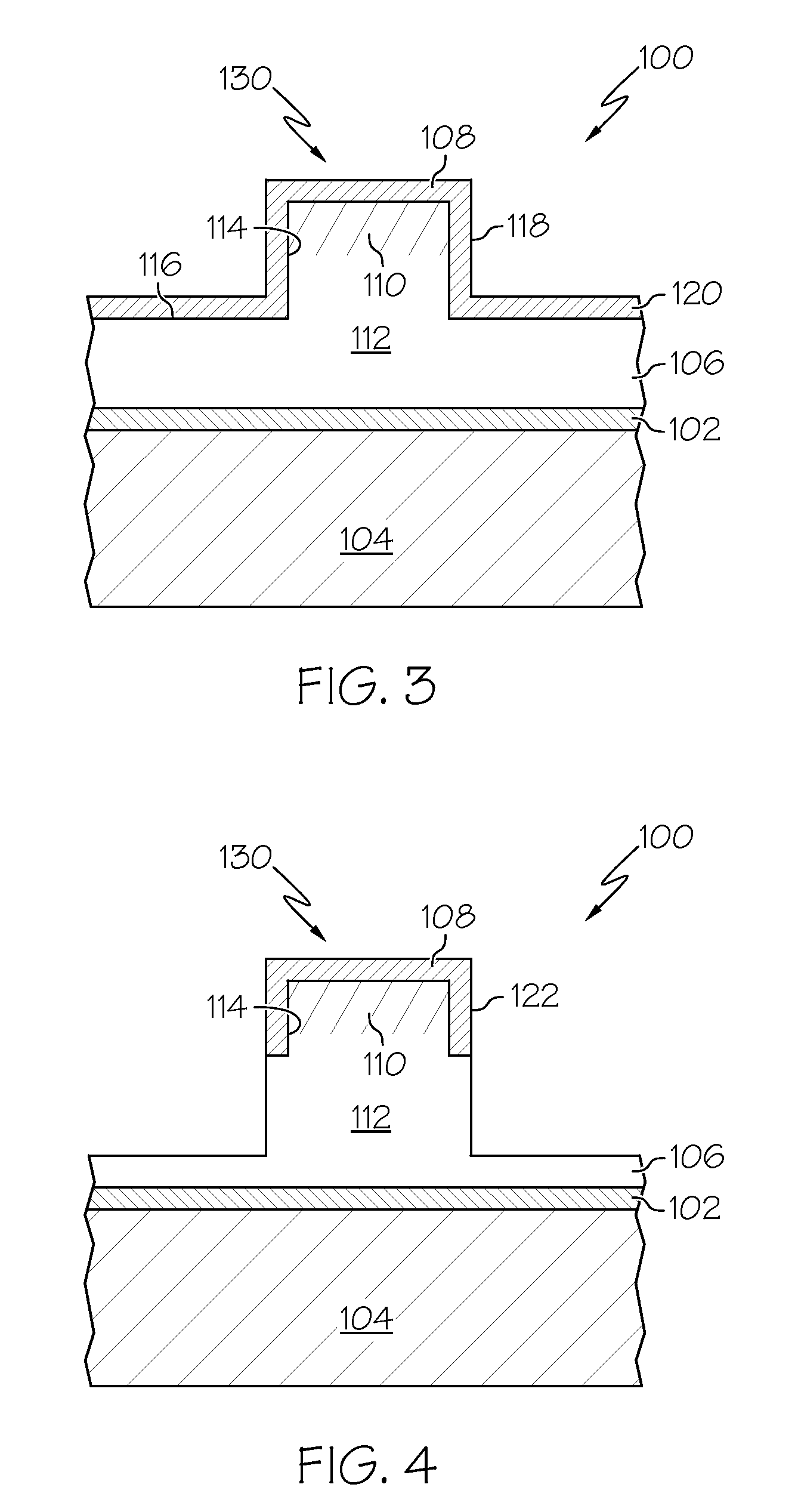
[0011]FIGS. 1-6 illustrate, in cross section, methods for forming a semiconductor device 100 in accordance with various embodiments of the invention. For illustrative purposes only, device 100 is depicted as an MOS transistor, and the focus of the description of embodiments is on a gate electrode structure 130 of the transistor. The invention is not limited to MOS transistors or to gate electrodes, but rather can be applied to the fabrication of any semiconductor device that employs a polycrystalline silicon device element such as a gate electrode, a conductive interconnect, or the like. Again, as stated above, the term “polycrystalline” i...
PUM
 Abstract
Description
Claims
Application Information