Nuclear batteries

a technology of nuclear batteries and batteries, applied in the field of nuclear batteries, can solve the problems of increasing power density, large device surface area, adding complexity and cost,

Active Publication Date: 2012-03-13
WIDETRONIX
View PDF4 Cites 28 Cited by
  • Summary
  • Abstract
  • Description
  • Claims
  • Application Information

AI Technical Summary

Problems solved by technology

Increasing power density is a difficult problem because, while both the active area of the semiconductor used for the beta energy conversion and the layer of radioisotope that provides the betas for this conversion are very thin (100's of nanometers), the thickness of the substrate supporting the radioisotope layer and the overall thickness of the semiconductor device wafers are on the order of 100's of microns.
Secondly, in order to produce high power density in betavoltaics, a large device surface area is required.
Because of such high temperature requirements, these epitaxial processes add an element of complexity and cost, not seen with processes relating to other semiconductors, such as Si, and must be taken into account accordingly, or fabrication techniques must be developed to remove such complex and costly processes entirely.

Method used


Image

  • Nuclear batteries
  • Nuclear batteries
  • Nuclear batteries

Examples


an embodiment

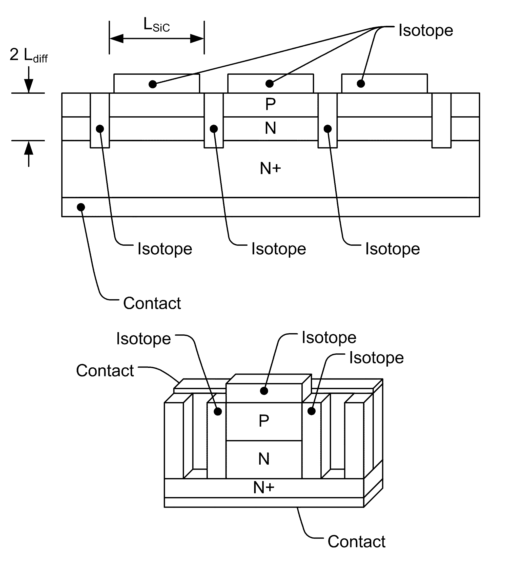
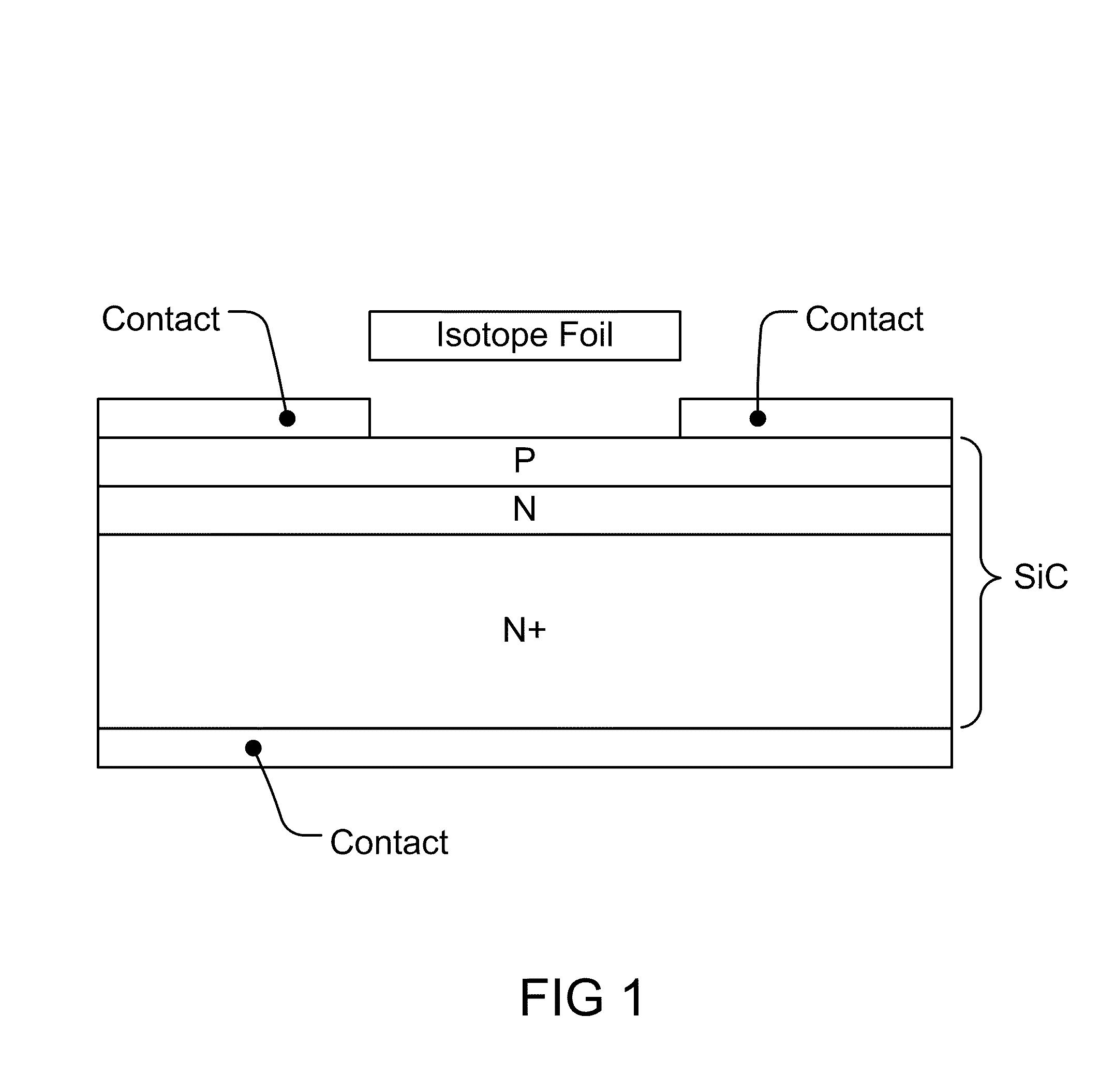
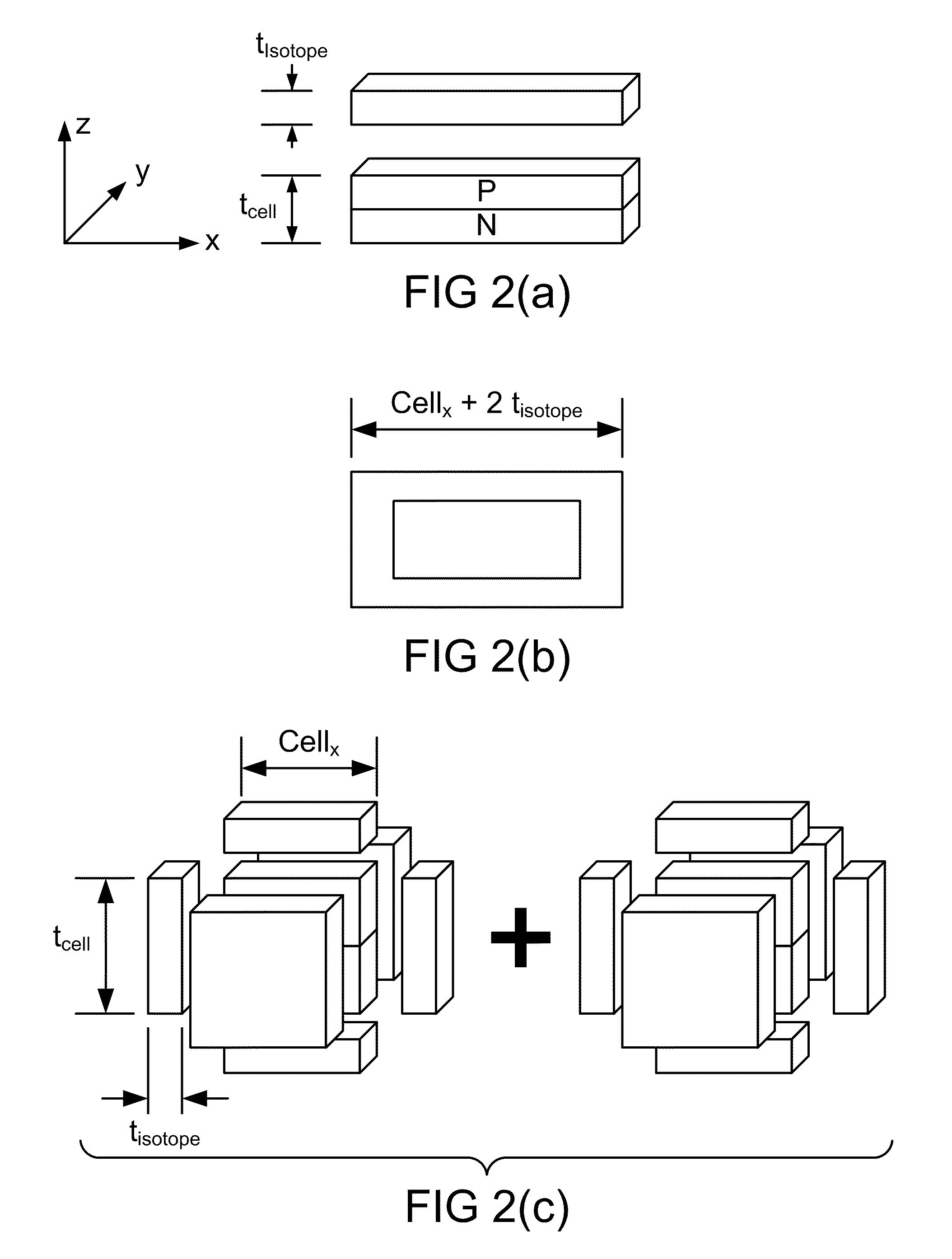
[0046]One embodiment of the invention is shown in FIG. 2. While the invention can be implemented with multiple junctions, this first embodiment will be described using a single junction. The top part of FIG. 2 shows the starting geometry which can be viewed as a combination of two slabs—a radioisotope slab and a SiC converter slab. The top slab (shown in red) is the radioisotope slab, and the bottom slab (shown in blue and yellow) is the PN junction slab. The top surface cross sectional dimensions (not shown) of the semiconductor slab are cellx and celly in the x and y directions respectively, and the z dimension (the thickness of the junction, also not shown) is denoted by tcell. In one example, we introduce additional isotope slabs to completely surround up to all four sides of the PN junction slab plus one isotope slab covering the junction slab's bottom or top surface or two additional slabs covering both the top and bottom junction surface. Multiple, and typically thousands, of...


PUM


Abstract

We introduce a new technology for Manufacturable, High Power Density, High Volume Utilization Nuclear Batteries. Betavoltaic batteries are an excellent choice for battery applications which require long life, high power density, or the ability to operate in harsh environments. In order to optimize the performance of betavoltaic batteries for these applications or any other application, it is desirable to maximize the efficiency of beta particle energy conversion into power, while at the same time increasing the power density of an overall device. The small (submicron) thickness of the active volume of both the isotope layer and the semiconductor device is due to the short absorption length of beta electrons. The absorption length determines the self absorption of the beta particles in the radioisotope layer as well as the range, or travel distance, of the betas in the semiconductor converter which is typically a semiconductor device comprising at least one PN junction. Various devices and methods to solve the current industry problems and limitations are presented here.

Description

RELATED APPLICATIONS[0001]This current application is a continuation-in-part of (and related to) U.S. application Ser. Nos. 12 / 888,521 filed Sep. 23, 2010, now U.S. Pat. No. 8,017,412 and 12 / 851,555, filed Aug. 6, 2010, which are based on the provisional applications 61 / 250,504, filed Oct. 10, 2009, 61 / 231,863, filed Aug. 6, 2009, and 61 / 306,541, filed Feb. 21, 2010, with common inventor(s), and same assignee (Widetronix Corporation). All of the above teachings are incorporated by reference here.BACKGROUND OF THE INVENTION[0002]We introduce a new technology for Manufacturable, High Power Density, High Volume Utilization Nuclear Batteries. Betavoltaic batteries are an excellent choice for battery applications which require long life, high power density, or the ability to operate in harsh environments. In order to optimize the performance of betavoltaic batteries for these applications or any other application, it is desirable to maximize the efficiency of beta particle energy convers...

Claims


Application Information

Patent Timeline
Patent Type & Authority Patents(United States)
IPC IPC(8): H01L27/14
CPCG21H1/02
Inventor SPENCER, MICHAELCHANDRASHEKHAR, MVSTHOMAS, CHRIS
Owner WIDETRONIX
Why Eureka
Try Eureka