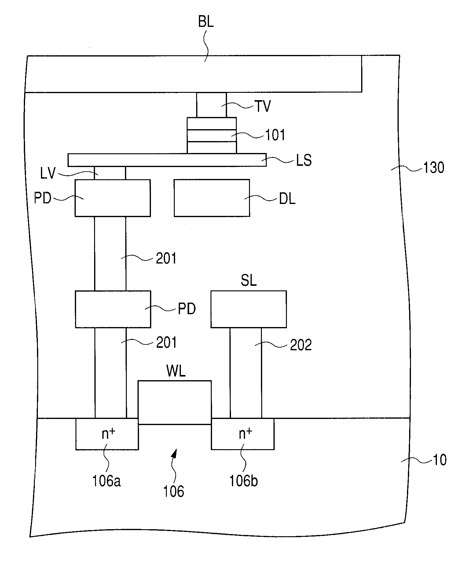
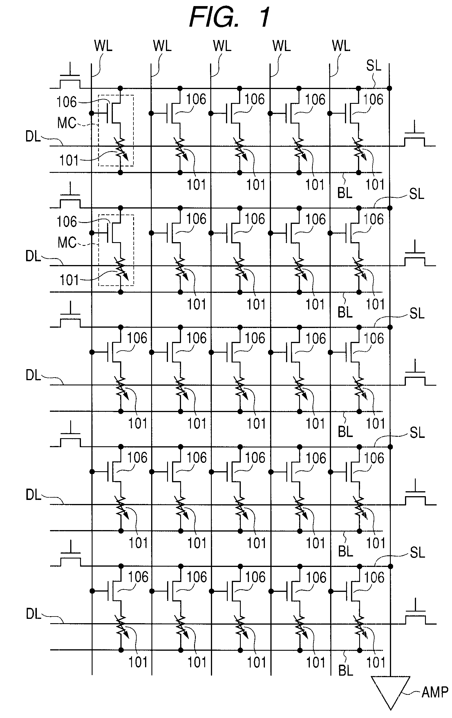
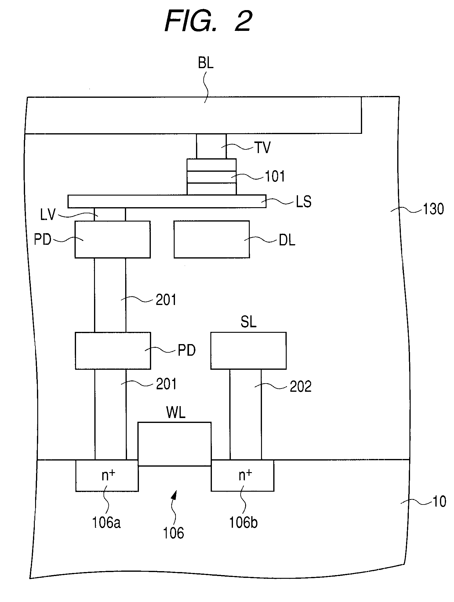
Magnetic memory device
a magnetic memory and lv technology, applied in semiconductor devices, digital storage, instruments, etc., can solve the problems of difficult process of flattening the principal surface of ls with lv coupled thereto, and achieve the effect of suppressing the increase in the occupied area of the strap wiring and suppressing the size of the magnetic memory devi
- Summary
- Abstract
- Description
- Claims
- Application Information
AI Technical Summary
Benefits of technology
Problems solved by technology
Method used
Image

Examples
first embodiment
[0075]In this embodiment, each TMR element 101 (or each recording layer 13) has the asymmetric shape illustrated in FIG. 4 as viewed on a plane. That is, at least each recording layer 13 has the asymmetric shape illustrated in FIG. 4. The following description is on the assumption that the planar shape of the entire TMR element 101 is this asymmetric shape.
[0076]As illustrated in FIG. 4, the TMR element 101 is asymmetric with respect to the easy magnetization axis S. It has the symmetric property with respect to the axis of symmetry (that can be understood as the direction of hard magnetization axis) L perpendicular to the easy magnetization axis S. The shape illustrated in FIG. 4 can be understood as crescent shape or fava bean shape. That is, in the asymmetric shape illustrated in FIG. 4 as an example, one contoured portion s1 of the TMR element 101 opposed to the easy magnetization axis S has such an outline that the following is implemented: it is concave inward of the TMR eleme...
second embodiment
[0108]In this embodiment, the TMR element 101 (or the recording layer 13) has the asymmetric shape illustrated in FIG. 16 as viewed on a plane. That is, at least the recording layer 13 has the asymmetric shape illustrated in FIG. 16. The following description is on the assumption that the planar shape of the entire TMR element 101 is this asymmetric shape.
[0109]As illustrated in FIG. 16, the TMR element 101 is asymmetric with respect to the easy magnetization axis S. It has the symmetric property with respect to the axis of symmetry (that can be understood as the direction of hard magnetization axis) L perpendicular to the easy magnetization axis S. That is, in the asymmetric shape illustrated in FIG. 16 as an example, one contoured portion 804 of the TMR element 101 opposed to the easy magnetization axis S has a linear shape. Meanwhile, the other contoured portion 801 of the TMR element 101 opposed to the easy magnetization axis S has such an outline that it is convex outward of th...
third embodiment
[0132]In this embodiment, the TMR element 101 (or the recording layer 13) has the asymmetric shape illustrated in FIG. 21 as viewed on a plane. That is, at least the recording layer 13 has the asymmetric shape illustrated in FIG. 21. The following description is on the assumption that the planar shape of the entire TMR element 101 is this asymmetric shape.
[0133]As illustrated in FIG. 21, the TMR element 101 is asymmetric with respect to the easy magnetization axis S. It has the symmetric property with respect to the axis of symmetry (that can be understood as the direction of hard magnetization axis) L perpendicular to the easy magnetization axis S. That is, in the asymmetric shape illustrated in FIG. 21 as an example, one contoured portion 850 of the TMR element 101 opposed to the easy magnetization axis S has such an outline that the following is implemented: it is convex outward of the TMR element 101 (to the left side of FIG. 21) with a first curvature. Meanwhile, the other cont...
PUM
 Abstract
Description
Claims
Application Information
 - R&D
- Intellectual Property
- Life Sciences
- Materials
- Tech Scout
- Unparalleled Data Quality
- Higher Quality Content
- 60% Fewer Hallucinations
Browse by: Latest US Patents, China's latest patents, Technical Efficacy Thesaurus, Application Domain, Technology Topic, Popular Technical Reports.
© 2025 PatSnap. All rights reserved.Legal|Privacy policy|Modern Slavery Act Transparency Statement|Sitemap|About US| Contact US: help@patsnap.com