Display Device and Method for Manufacturing the Same

a technology of display device and manufacturing method, which is applied in the field of display device, can solve the problems of reducing the performance of the other, and achieve the effects of excellent electrical and physical characteristics, high image quality, and high performan

Inactive Publication Date: 2018-02-01
SEMICON ENERGY LAB CO LTD
View PDF1 Cites 6 Cited by
  • Summary
  • Abstract
  • Description
  • Claims
  • Application Information

AI Technical Summary

Benefits of technology

[0037]Since a transmissive display element and a reflective display element in each of which the material and the thickness are optimized can be each driven by a transistor having required excellent electrical and physical characteristics, a display device having high-image quality and high performance can be provided. In addition, since the transmissive display element and the reflective display element are stacked between a pair of substrates, an increase in the size of the display device can be suppressed.

Problems solved by technology

However, the transmissive mode and the reflective mode have different characteristics and optimal conditions, and thus there is a problem in that when the optimal conditions of one of the transmissive mode and the reflective mode have higher priority, the performance of the other is reduced.

Method used


Image

  • Display Device and Method for Manufacturing the Same
  • Display Device and Method for Manufacturing the Same
  • Display Device and Method for Manufacturing the Same

Examples


embodiment 1

[0061]Embodiments of a display device and a method for manufacturing the display device are described with reference to FIG. 1, FIGS. 2A to 2H, FIGS. 3A to 3C, FIG. 4, FIG. 5, FIGS. 6A1 to 6E, FIGS. 7A1 to 7E, and FIG. 8.

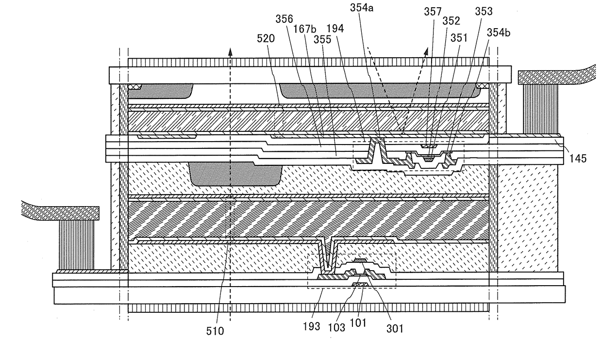
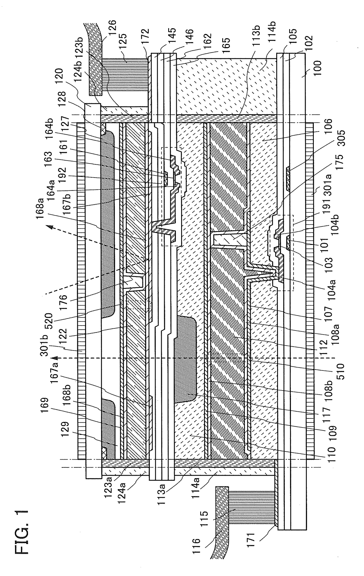
[0062]FIG. 1 is a cross-sectional view of one embodiment of a display device. In the display device in FIG. 1, a circularly polarizing plate 301a; a first substrate 100 having a light-transmitting property; a transistor 191 including a gate electrode layer 101, a gate insulating film 102, a semiconductor film 103, and wiring layers 104a and 104b serving as a source electrode layer and a drain electrode layer; a light-blocking film 305 which protects a transistor 192 from light from a backlight which can be used as a light source; an insulating film 105; an insulating film 106 serving as a planarization film; a first pixel electrode layer 107; an insulating film 108a serving as an alignment film; a spacer 175; a first liquid crystal 112; an insulating film 108b servi...

embodiment 2

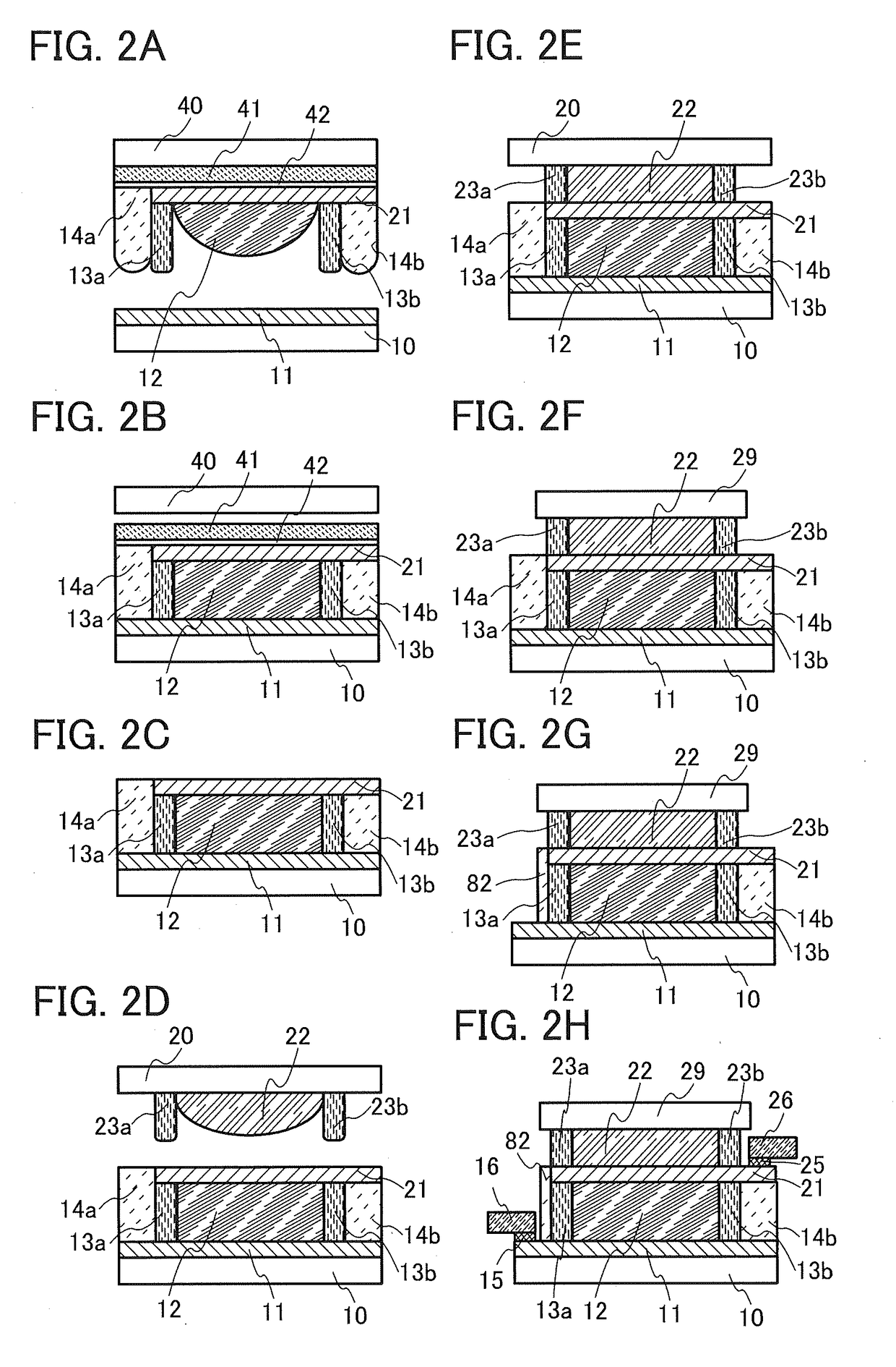
[0180]One embodiment of a method for manufacturing the display device in FIG. 1 or the like is described with reference to FIGS. 9A to 9G. Note that in FIGS. 9A to 9G, the circularly polarizing plate, the alignment film, the pixel electrode layer, the counter electrode layer, and the like are omitted for simplicity. The method in this embodiment is a modification example of the manufacturing method illustrated in FIGS. 2A to 2H in Embodiment 1. Accordingly, portions which are the same as or have functions similar to those in Embodiment 1 are denoted by the same reference numerals in different drawings, and Embodiment 1 can be referred to for the portions; therefore, descriptions thereof are not repeated.

[0181]As described with reference to FIGS. 2A and 2B in Embodiment 1, using the sealants 13a and 13b and the resin layers 14a and 14b, the first substrate 10 over which the first pixel electrode layer and the layer 11 including the transistor are formed and the manufacturing substrat...

embodiment 3

[0200]In this embodiment, a structure of a data processing device of one embodiment of the invention disclosed in this specification is described with reference to FIGS. 10A to 10C, FIGS. 11A and 11B, and FIG. 12.

[0201]FIG. 10A is a block diagram illustrating a structure of a data processing device of one embodiment of the invention disclosed in this specification. FIGS. 10B and 10C are projection views illustrating examples of external views of a data processing device 200.

[0202]FIGS. 11A and 11B are flow charts illustrating a program of one embodiment of the invention disclosed in this specification. FIG. 11A is a flow chart showing main processing of the program of one embodiment of the invention disclosed in this specification, and FIG. 11B is a flow chart showing interrupt processing.

[0203]FIG. 12 is a flow chart illustrating interrupt processing of a program of one embodiment of the invention disclosed in this specification.

[0204]The data processing device 200 described in thi...


PUM

PropertyMeasurementUnit
sizeaaaaaaaaaa
thicknessaaaaaaaaaa
thicknessaaaaaaaaaa

Abstract

A high-image-quality display device having a transmissive mode and a reflective mode is provided. Furthermore, the display device is manufactured with higher yield and higher productivity. In the display device, a transistor used for a transmissive liquid crystal display element, the transmissive liquid crystal display element, a transistor used for a reflective liquid crystal display element, and the reflective liquid crystal display element are stacked in this order between a pair of substrates. In a manufacturing process, one or two manufacturing substrates are used in addition to the pair of substrates included in the display device. The display device is manufactured in such a manner that a second liquid crystal and a second sealant provided to surround the second liquid crystal are bonded to a first liquid crystal sealed using a first sealant. The bonding process is performed such that the first sealant and the second sealant overlap with each other. Moreover, an end portion of the first sealant which is in contact with the first liquid crystal is substantially aligned with or positioned closer to the inner side of the display device than an end portion of the second sealant which is in contact with the second liquid crystal.

Description

BACKGROUND OF THE INVENTION1. Field of the Invention[0001]The present invention relates to a display device and a method for manufacturing the display device.2. Description of the Related Art[0002]In recent years, liquid crystals have been applied to a variety of devices; in particular, liquid crystal display devices (liquid crystal displays) having advantages of thinness and lightness have been used for displays in a wide range of fields.[0003]There are two types of liquid crystal display devices: a transmissive mode liquid crystal display device using light from a backlight and a reflective mode liquid crystal display device using reflected light obtained by reflection of external light. In addition, transflective liquid crystal display devices having a transmissive mode and a reflective mode have been proposed. Patent Document 1 discloses a transflective liquid crystal display device including a transmissive region and a reflective region in one pixel.REFERENCEPatent Document[000...

Claims


Application Information

Patent Timeline
Patent Type & Authority Applications(United States)
IPC IPC(8): G02F1/1345G02F1/1335G02F1/1362G02F1/1343G02F1/1368G02F1/1339
CPCG02F1/1345G02F1/1368G02F1/1339G02F1/136286G02F2203/02G02F1/13439G02F1/133553G02F2201/123G02F2203/01G02F1/134309G02F1/133555G02F1/1347
Inventor KUBOTA, DAISUKEKUSUNOKI, KOJIYAMASHITA, AKIO
Owner SEMICON ENERGY LAB CO LTD
Why Eureka
Try Eureka