

Three-dimensional semiconductor devices
a semiconductor device and three-dimensional technology, applied in the field of three-dimensional semiconductor devices, can solve the problems of limited increase in integration of two-dimensional memory devices, etc., and achieve the effect of increasing integration
- Summary
- Abstract
- Description
- Claims
- Application Information
AI Technical Summary
Benefits of technology
Problems solved by technology
Method used
Image

Examples
Embodiment Construction
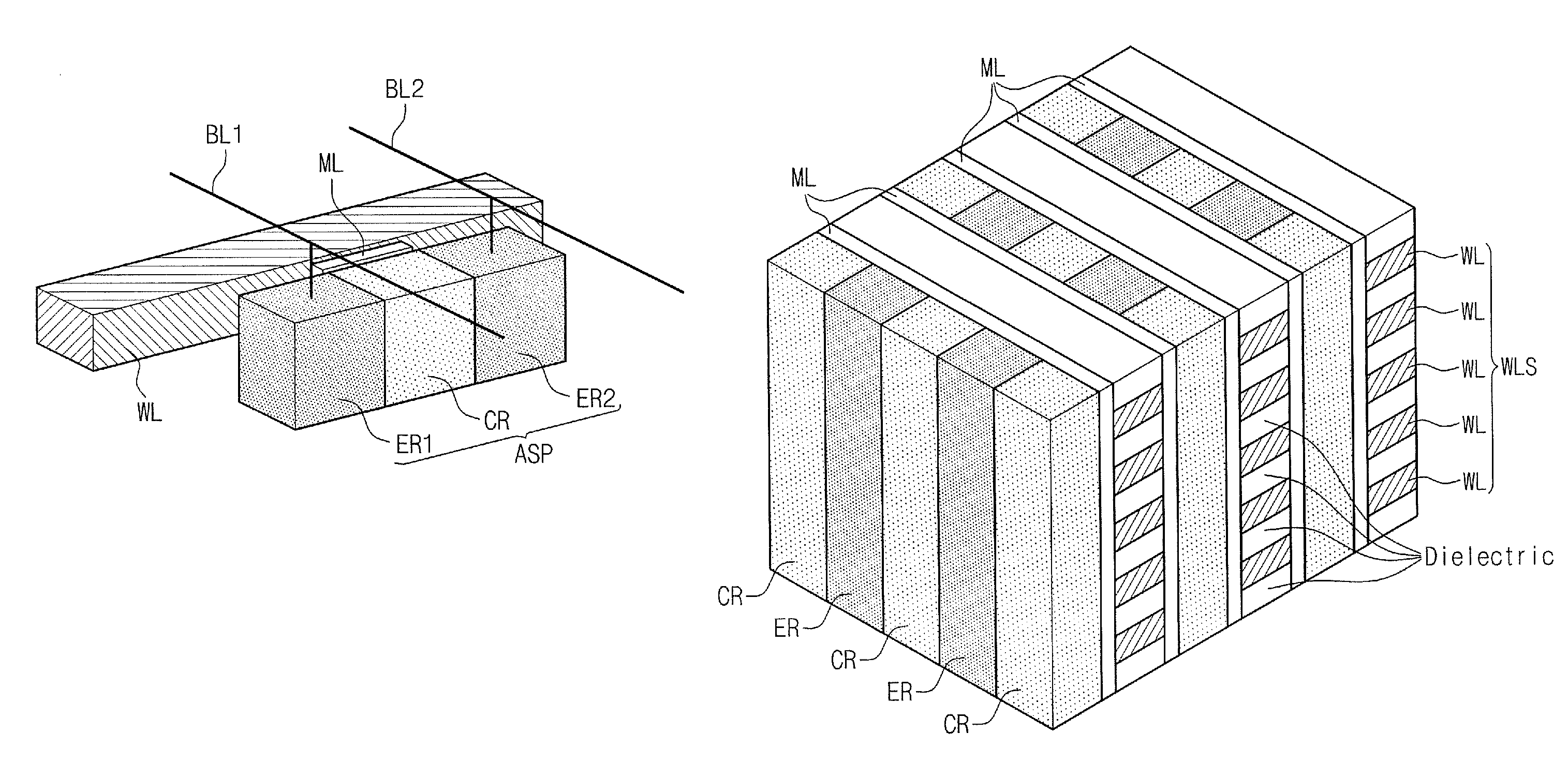
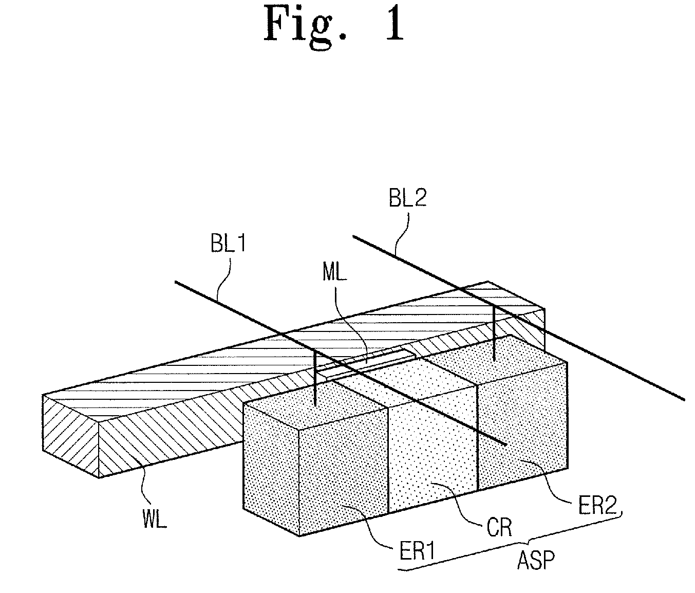
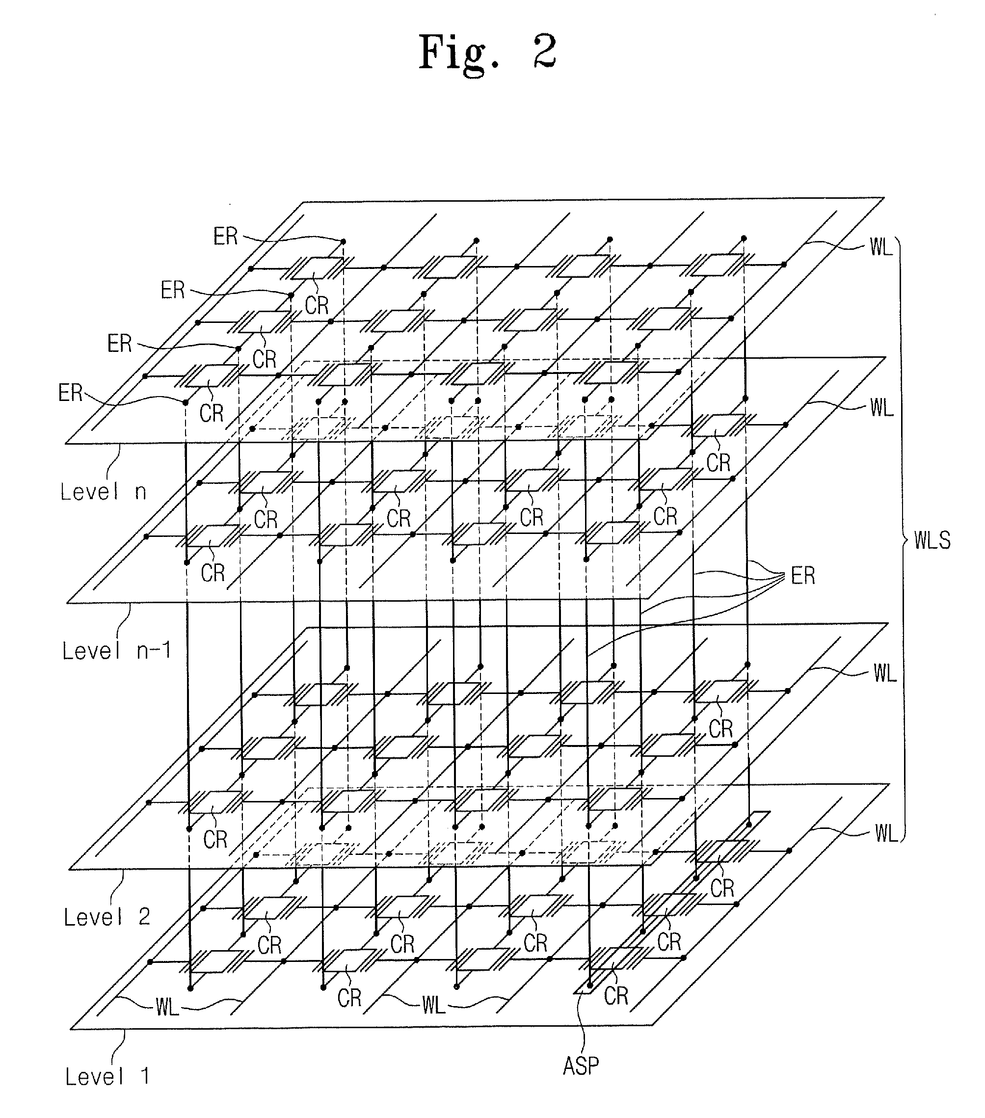
[0053]The present invention now will be described more fully hereinafter with reference to the accompanying drawings, in which embodiments of the invention are shown. However, this invention should not be construed as limited to the embodiments set forth herein. Rather, these embodiments are provided so that this disclosure will be thorough and complete, and will fully convey the scope of the invention to those skilled in the art.
[0054]It will be understood that, although the terms first, second, etc. may be used herein to describe various elements, these elements should not be limited by these terms. These terms are only used to distinguish one element from another element. Thus, a first element discussed below could be termed a second element without departing from the scope of the present invention. In addition, as used herein, the singular forms “a”, “an” and “the” are intended to include the plural forms as well, unless the context clearly indicates otherwise. It also will be u...
PUM
 Abstract
Description
Claims
Application Information