

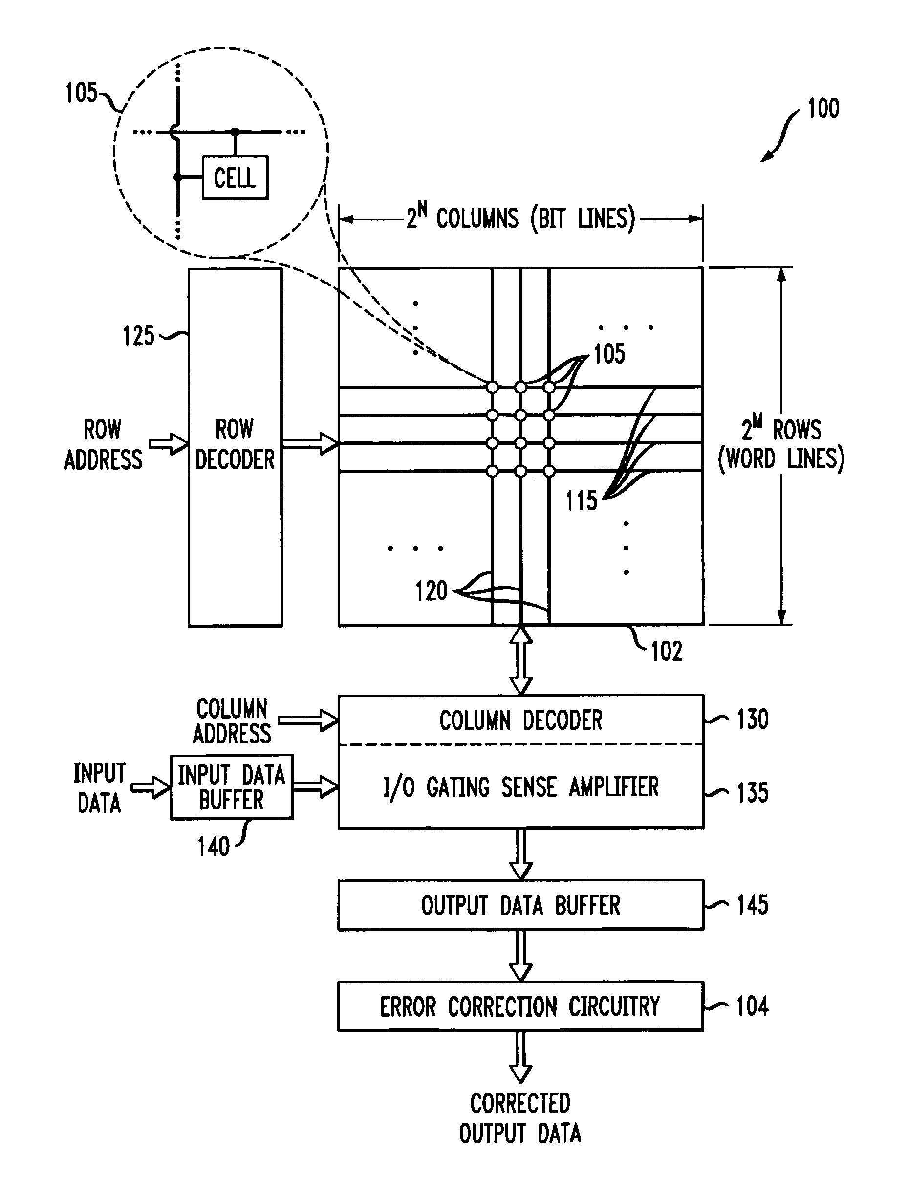
Memory device with error correction capability and efficient partial word write operation
a memory device and partial word technology, applied in error detection/correction, digital storage, instruments, etc., can solve the problems of reducing the yield of the integrated circuit manufacturing process, reducing the data transfer rate of the memory device, and causing the error of the memory cell to be read with incorrect data
- Summary
- Abstract
- Description
- Claims
- Application Information
AI Technical Summary
Benefits of technology
Problems solved by technology
Method used
Image

Examples
case 1
[0061]Case 1 corresponds to the situation previously described in conjunction with FIG. 5, where a partial word write operation comprising a read phase and a write phase is followed by a read operation. It appears externally to the memory device as if the partial word write operation and the read operation occur in respective single consecutive cycles, although internally the write phase of the partial word write operation is multiplexed with the read operation in the manner illustrated in FIG. 5.
case 2
[0062]Case 2 corresponds to a partial word write operation followed by a write operation. A write operation cannot occur simultaneously with another write operation or write phase. For this reason, a write operation requested in the second cycle of a partial word write operation must be delayed until the following clock cycle, which is the third cycle in the present example. If a read operation has been requested for the third cycle, the write operation will occur simultaneously with the read operation during the third cycle. If a partial word write operation is requested for the third cycle, the write operation will occur simultaneously with the read phase of the partial word write operation. If another write operation is requested as the third cycle, this new write operation will be delayed until the fourth cycle.
case 3
[0063]Case 3 corresponds to a situation in which a partial word write operation is followed by another partial word write operation. Because the read phase is the first phase of a partial word write operation, a partial word write operation followed by another partial word write operation is very similar to a partial word write operation followed by a read operation. Thus, the situation is similar to that shown in FIG. 5, with the read operation being replaced with the read phase of the second partial word write.
PUM
 Abstract
Description
Claims
Application Information