Circuit board structure and method for manufacturing the same

a technology of circuit board and structure, applied in the field of circuit board, can solve the problems of circuit layer damage, inability to achieve stable quality of circuit layer, etc., and achieve the effect of controlling circuits and advancing electric performances

Active Publication Date: 2012-04-17
UNIMICRON TECH CORP
View PDF1 Cites 2 Cited by
  • Summary
  • Abstract
  • Description
  • Claims
  • Application Information

AI Technical Summary

Benefits of technology

[0009]In view of the above conventional shortcomings, the object of the present invention is to provide a circuit board structure and a method for manufacturing the same so as to control circuits in predetermined shape efficiently, to form circuit boards having fine circuits, and to advance the electric performances of circuit boards in the same time.
[0011]Because the surfaces of the second circuit layer, the conductive vias, and the dielectric layer are on the same plane, circuits can be ensured in predetermined shape so that the circuit board can have fine circuits.
[0014]In the above-mentioned circuit board structure, a substrate serves as a core of the core board, and the first circuit layer is formed on the surfaces of the substrate in which a plurality of plated through holes are formed and conduct to the first circuit layer formed on the surfaces of the substrate. Moreover, the number of layers in the core board is not limited to, but the core board can be double-sided circuit board or a multilayer circuit board. Nowadays, dielectric materials are generally filled with fillers in a large dimension (max=10 μm). This kind of dielectric material is disadvantageous to manufacture fine circuits, i.e. line width and line space are respectively smaller than 15 μm. However, the dielectric layer in the present invention is made of a photosensitive dielectric material having high resistivity so that electromigration or point discharge due to line space decreased can be moderated efficiently. Additionally, the dielectric layer can be processed by exposure and development to form openings. The photosensitive dielectric material can selectively further comprise at least one fine particle filler or without any filler so as to benefit fine circuit manufacturing.

Problems solved by technology

Accordingly, the required stable quality of the circuit layer can not be achieved.
In addition, inappropriate narrow circuits are manufactured under unstable manufacturing processes resulting in circuits being damaged.

Method used


Image

  • Circuit board structure and method for manufacturing the same
  • Circuit board structure and method for manufacturing the same
  • Circuit board structure and method for manufacturing the same

Examples


embodiment 1

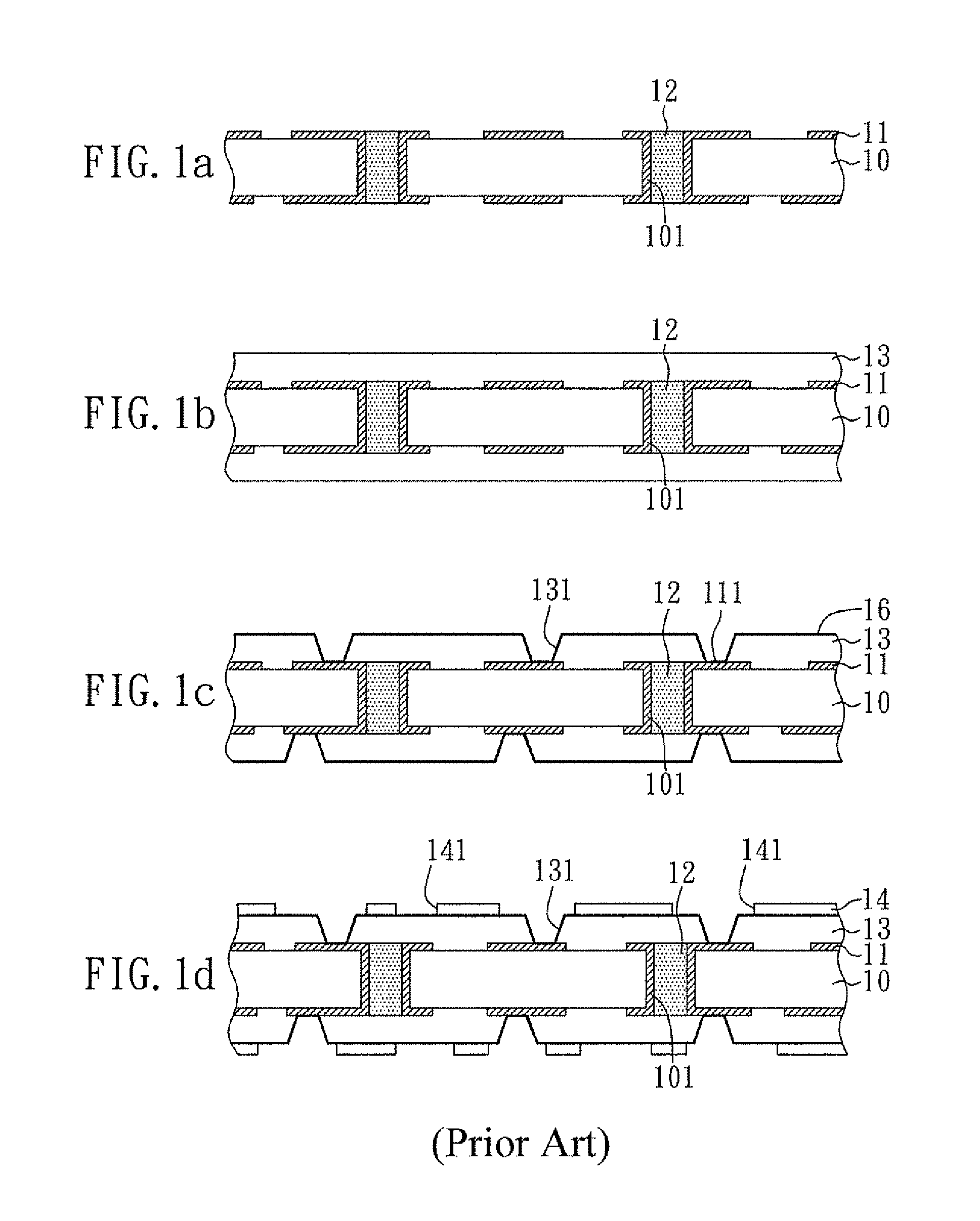
[0027]With reference to FIGS. 2a to 2h, there is shown a flow chart of the method for manufacturing a circuit board structure in Embodiment 1 of the present invention.

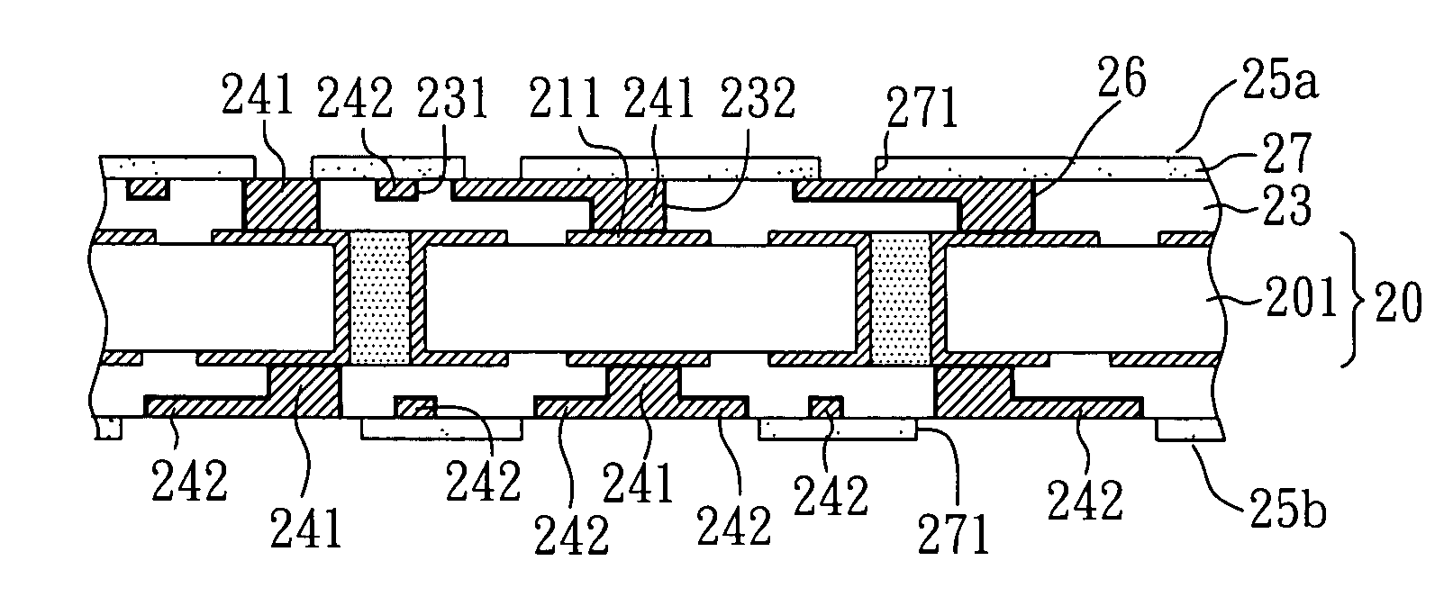
[0028]As shown in FIG. 2a, a core board 20 is provided. The core board 20 has a first circuit layer 21 respectively on the upper and lower surface. Besides, the first circuit layer 21 has a plurality of conductive pads 211. Therefore, the core board used in the present embodiment can be a double-sided circuit board or a multilayer circuit board, which has the first circuit layer 21. Besides, a substrate 201 serves as a core of the core board 20, and the first circuit layer 21 is formed on the upper and lower surfaces of the substrate 201 in which a plurality of plated through holes 202 are formed. The first circuit layer 21 formed on the surfaces of the substrate 201 is conducted with the plated through holes 202. In addition, the plated through holes 202 are filled with resin 22.

[0029]As shown in FIG. 2b, a dielectric...


PUM

PropertyMeasurementUnit
conductiveaaaaaaaaaa
photosensitiveaaaaaaaaaa
resistivityaaaaaaaaaa

Abstract

A circuit board disclosed in the present invention includes a core board on which a first circuit layer is placed, wherein the first circuit layer has a plurality of conductive pads; and at least one built-up structure covering the surface of the circuit board, which comprises a dielectric layer, a second circuit layer, and a plurality of conductive vias without being surrounded by annular metal rings. The conductive vias are conducted with the conductive pads of the first circuit layer and the second circuit layer. Besides, the surface of the second circuit layer is in the same height as the surface of the dielectric layer. Also, the present invention provides a method for manufacturing the above-mentioned circuit board structure. Therefore, a circuit board having fine circuits can be formed, and the shape of the circuit can be ensured efficiently. Moreover, electric performances of the circuit board can be improved.

Description

BACKGROUND OF THE INVENTION[0001]1. Field of the Invention[0002]The present invention relates to a circuit board and a method for manufacturing the same, and, especially, to a circuit board having fine circuits and a method for manufacturing the same.[0003]2. Description of Related Art[0004]Customer demands of the electronics industry continue to evolve rapidly and the main trends are high integration and miniaturization. In order to satisfy those requirements, especially in the packaging of semiconductor devices, development of circuit boards with the maximum of active and passive components and conductive circuit layers has progressed from double-layer to multi-layer types. This means that a greater circuit layout area is available due to interlayer connection technology so that the requirement of high-density integrated circuits can be satisfied. Therefore, the thickness of package substrates will be lessened, and more circuits and electric components can be included in the packa...

Claims


Application Information

Patent Timeline
Patent Type & Authority Patents(United States)
IPC IPC(8): H05K1/11
CPCH05K3/465H05K3/0023H05K3/0035Y10T29/49155H05K2201/0376H05K3/045
Inventor SHIH, CHAO-WEN
Owner UNIMICRON TECH CORP
Why Eureka
Try Eureka